SBVS228B July 2013 – March 2015 TPS7A3501
PRODUCTION DATA.
- 1 Features
- 2 Applications
- 3 Description
- 4 Revision History
- 5 Pin Configuration and Functions
- 6 Specifications
- 7 Detailed Description
- 8 Application and Implementation
- 9 Power Supply Recommendations
- 10Layout
- 11Device and Documentation Support
- 12Mechanical, Packaging, and Orderable Information
パッケージ・オプション
メカニカル・データ(パッケージ|ピン)
- DRV|6
サーマルパッド・メカニカル・データ
- DRV|6
発注情報
6 Specifications
6.1 Absolute Maximum Ratings
over operating junction temperature range (unless otherwise noted).(1)| MIN | MAX | UNIT | ||
|---|---|---|---|---|
| Voltage | IN, NR, EN | –0.3 | 7 | V |
| OUT, SENSE | –0.3 | VIN + 0.3(2) | ||
| Current | OUT | Internally limited | ||
| Temperature | Operating junction, TJ | –40 | 125 | °C |
| Storage, Tstg | –55 | 150 | ||
(1) Stresses beyond those listed under Absolute Maximum Ratings may cause permanent damage to the device. These are stress ratings only, which do not imply functional operation of the device at these or any other conditions beyond those indicated under Recommended Operating Conditions. Exposure to absolute-maximum-rated conditions for extended periods may affect device reliability.
(2) Absolute maximum rating is VIN + 0.3 V or + 7 V, whichever is smaller.
6.2 ESD Ratings
| VALUE | UNIT | |||
|---|---|---|---|---|
| V(ESD) | Electrostatic discharge | Human body model (HBM), per ANSI/ESDA/JEDEC JS-001, all pins(1) | ±1000 | V |
| Charged device model (CDM), per JEDEC specification JESD22-C101, all pins(2) | ±250 | |||
(1) JEDEC document JEP155 states that 500-V HBM allows safe manufacturing with a standard ESD control process.
(2) JEDEC document JEP157 states that 250-V CDM allows safe manufacturing with a standard ESD control process.
6.3 Recommended Operating Conditions
over operating junction temperature range (unless otherwise noted).| MIN | NOM | MAX | UNIT | ||
|---|---|---|---|---|---|
| VIN | Input voltage | 1.71 | 5 | V | |
| IOUT | Output current | 0 | 1 | A | |
| TJ | Operating junction temperature | –40 | 125 | °C | |
6.4 Thermal Information
| THERMAL METRIC(1) | DRV (WSON) | UNIT | |
|---|---|---|---|
| 6 PINS | |||
| RθJA | Junction-to-ambient thermal resistance | 66.9 | °C/W |
| RθJC(top) | Junction-to-case (top) thermal resistance | 86.5 | |
| RθJB | Junction-to-board thermal resistance | 36.4 | |
| ψJT | Junction-to-top characterization parameter | 1.8 | |
| ψJB | Junction-to-board characterization parameter | 36.6 | |
| RθJC(bot) | Junction-to-case (bottom) thermal resistance | 7.3 | |
(1) For more information about traditional and new thermal metrics, see the IC Package Thermal Metrics application report, SPRA953.
6.5 Electrical Characteristics
At TJ = –40°C to 125°C, VIN = 3.6 V, RNR = ∞ (not connected), IOUT = 10 mA, VEN = VIN, and CIN = COUT = 10 µF, unless otherwise noted.| PARAMETER | TEST CONDITIONS | MIN | TYP | MAX | UNIT | |
|---|---|---|---|---|---|---|
| VIN | Input voltage range | 1.71 | 5 | V | ||
| VUVLO(in) | Input supply UVLO | VIN increasing | 1.5 | 1.7 | V | |
| VIN hysteresis | 200 | mV | ||||
| VOUT | Output voltage range | 1.21 | 4.5 | V | ||
| VIN – VOUT voltage range | 200 | 500 | mV | |||
| VOUT(nom) = VIN – 330 mV, IOUT ≤ 1 A, 1.71 V ≤ VIN ≤ 4.83 V |
297 | 330 | 363 | mV | ||
| RNR_INTERNAL(1) | 110 | 170 | 210 | kΩ | ||
| INR_INTERNAL(2) | 1.4 | 1.8 | 2.4 | µA | ||
| ∆VOUT(∆IOUT) | Load regulation | 10 mA ≤ IOUT ≤ 1 A | 10 | µV/mA | ||
| ICL | Output current limit | VOUT = 0.85 × VOUT(nom) | 1.1 | A | ||
| IGND | GND pin current | 2.25 | 5 | mA | ||
| IEN | EN pin input current | VEN = VIN | 1 | 50 | nA | |
| ISHUTDOWN | Shutdown current (IGND) | VEN ≤ 0.3 V | 0.01 | 3 | µA | |
| PSRR | Power-supply rejection ratio | f = 10 kHz, CNR = 1 µF, IOUT = 0.5 A | 55 | dB | ||
| f = 100 kHz, CNR = 1 µF, IOUT = 0.5 A | 40 | |||||
| f = 1 MHz, CNR = 1 µF, IOUT = 0.5 A | 42 | |||||
| Vn | Output noise voltage | BW = 10 Hz to 100 kHz, CNR = 1 µF, IOUT = 1 A | 3.8 | µVRMS | ||
| BW = 100 Hz to 100 kHz, CNR = 1 µF, IOUT = 1 A |
3.62 | |||||
| BW = 10 Hz to 1 MHz, CNR = 1 µF, IOUT = 1 A | 12.1 | |||||
| VEN(LO) | EN pin input low (disable) | 0.4 | V | |||
| VEN(HI) | EN pin input high (enable) | 1.1 | V | |||
| Tsd | Thermal shutdown junction temperature | Shutdown, temperature increasing | 165 | °C | ||
| Shutdown, temperature hysteresis | 20 | |||||
(1) RNR_INTERNAL refers to the internal resistor used to set (VIN – VOUT) for the device when no external RNR is used. See Adjustable Voltage Drop and Typical Application Circuitfor details.
(2) INR_INTERNAL refers to the internal current source used to set (VIN – VOUT) for the device when no external RNR is used. See Adjustable Voltage Drop and Typical Application Circuit for details.
6.6 Typical Characteristics
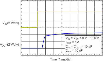
At VIN = 3.6 V, RNR = ∞ (not connected), IOUT = 10 mA, VEN = VIN, COUT = 10 µF, CIN = 10 µF, and CNR = 0.1 µF, unless otherwise noted.


