JAJSDJ7 August 2017 TPS7A47-Q1
PRODUCTION DATA.
- 1 特長
- 2 アプリケーション
- 3 概要
- 4 改訂履歴
- 5 Pin Configuration and Functions
- 6 Specifications
- 7 Detailed Description
- 8 Application and Implementation
- 9 Power Supply Recommendations
- 10Layout
- 11デバイスおよびドキュメントのサポート
- 12メカニカル、パッケージ、および注文情報
パッケージ・オプション
メカニカル・データ(パッケージ|ピン)
- RGW|20
サーマルパッド・メカニカル・データ
- RGW|20
発注情報
8 Application and Implementation
NOTE
Information in the following applications sections is not part of the TI component specification, and TI does not warrant its accuracy or completeness. TI’s customers are responsible for determining suitability of components for their purposes. Customers should validate and test their design implementation to confirm system functionality.
8.1 Application Information
The TPS7A47-Q1 is a high-voltage, low-noise, 1-A LDO. Low-noise performance makes this LDO ideal for providing rail voltages to noise-sensitive loads, such as PLLs, oscillators, and high-speed ADCs.
8.2 Typical Application
As shown in Figure 24, output voltage is set by grounding the appropriate control pins. When grounded, all control pins add a specific voltage on top of the internal reference voltage (V(REF) = 1.4 V). For example, when grounding pins 0P1V, 0P2V, and 1P6V, the voltage values 0.1 V, 0.2 V, and 1.6 V are added to the 1.4-V internal reference voltage for VO(nom) equal to 3.3 V, as described in the Programming section.
 Figure 24. Typical Application, VOUT = 3.3 V
8.2.1 Design Requirements
| PARAMETER | DESIGN REQUIREMENT |
|---|---|
| Input voltage | 5.0 V, ±10% |
| Output voltage | 3.3 V, ±3% |
| Output current | 500 mA |
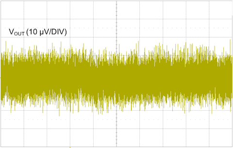
| Peak-to-peak noise, 10 Hz to 100 kHz | 50 µVPP |
8.2.2 Detailed Design Procedure
8.2.2.1 Capacitor Recommendations
This LDO is designed to be stable using low equivalent series resistance (ESR), ceramic capacitors at the input, output, and at the noise-reduction pin (NR, pin 14). Multilayer ceramic capacitors have become the industry standard for these types of applications and are recommended here, but must be used with good judgment. Ceramic capacitors that employ X7R-, X5R-, and COG-rated dielectric materials provide relatively good capacitive stability across temperature, but the use of Y5V-rated capacitors is discouraged precisely because the capacitance varies so widely. In all cases, ceramic capacitance varies a great deal with operating voltage and the design engineer must be aware of these characteristics. TI recommends applying a 50% derating of the nominal capacitance in the design.
Attention must be given to the input capacitance to minimize transient input droop during load current steps because the TPS7A47-Q1 has a very fast load transient response. Large input capacitors are necessary for good transient load response, and have no detrimental influence on the stability of the device. However, using large ceramic input capacitances can also cause unwanted ringing at the output if the input capacitor, in combination with the wire lead inductance, creates a high-Q peaking effect during transients. For example, a 5-nH lead inductance and a 10-µF input capacitor form an LC filter with a resonance frequency of 712 kHz at the edge of the control loop bandwidth. Short, well-designed interconnect leads to the up-stream supply minimize this effect without adding damping. Damping of unwanted ringing can be accomplished by using a tantalum capacitor, with a few hundred milliohms of ESR, in parallel with the ceramic input capacitor.
8.2.2.1.1 Input and Output Capacitor Requirements
The TPS7A47-Q1 is designed and characterized for operation with ceramic capacitors of 10 µF or greater at the input and output. Optimal noise performance is characterized using a total output capacitor value of 50 µF. Input and output capacitances must be located as near as practical to the respective input and output pins.
8.2.2.1.2 Noise-Reduction Capacitor (CNR)
The noise-reduction capacitor, connected to the NR pin of the LDO, forms an RC filter for filtering out noise that might ordinarily be amplified by the control loop and appear on the output voltage. Larger capacitances, up to 1 µF, affect noise reduction at lower frequencies and also tend to further reduce noise at higher frequencies. CNR also serves a secondary purpose in programming the turn-on rise time of the output voltage and thereby controls the turn-on surge current.
8.2.2.2 Dropout Voltage (VDO)
Generally speaking, the dropout voltage often refers to the voltage difference between the input and output voltage (V(DO) = VI – VO). However, in the Electrical Characteristics V(DO) is defined as the VI – VO voltage at the rated current (I(RATED)), where the main current pass-FET is fully on in the Ohmic region of operation and is characterized by the classic RDS(on) of the FET. V(DO) indirectly specifies a minimum input voltage above the nominal programmed output voltage at which the output voltage is expected to remain within its accuracy boundary. If the input falls below this V(DO) limit (VI < VO + V(DO)), then the output voltage decreases in order to follow the input voltage.
Dropout voltage is always determined by the RDS(on) of the main pass-FET. Therefore, if the LDO operates below the rated current, then V(DO) is directly proportional to the output current and can be reduced by the same factor. Use Equation 4 to calculate RDS(on) for the TPS7A47-Q1:

8.2.2.3 Output Voltage Accuracy
The output voltage accuracy specifies minimum and maximum output voltage error, relative to the expected nominal output voltage stated as a percent. This accuracy error typically includes the errors introduced by the internal reference and the load and line regulation across the full range of rated load and line operating conditions over temperature, unless otherwise specified by the Electrical Characteristics. Output voltage accuracy also accounts for all variations between manufacturing lots.
8.2.2.4 Startup
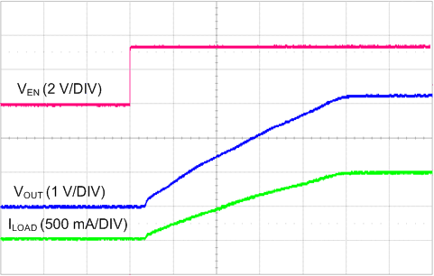
The startup time for the TPS7A47-Q1 depends on the output voltage and the capacitance of the CNR capacitor. Equation 5 calculates the startup time for a typical device.

where
- CNR = capacitance of the CNR capacitor
- VR = VO voltage if using the ANY-OUT configuration, or 1.4 V if using the adjustable configuration
8.2.2.5 AC Performance
AC performance of the LDO is typically understood to include power-supply rejection ratio, load step transient response, and output noise. These metrics are primarily a function of open-loop gain and bandwidth, phase margin, and reference noise.
8.2.2.5.1 Power-Supply Rejection Ratio (PSRR)
PSRR is a measure of how well the LDO control loop rejects ripple noise from the input source to make the dc output voltage as noise-free as possible across the frequency spectrum (usually 10 Hz to 10 MHz). Equation 6 gives the PSRR calculation as a function of frequency where input noise voltage [VS(IN)(f)] and output noise voltage [VS(OUT)(f)] are understood to be purely ac signals.

Noise that couples from the input to the internal reference voltage for the control loop is also a primary contributor to reduced PSRR magnitude and bandwidth. This reference noise is greatly filtered by the noise-reduction capacitor at the NR pin of the LDO in combination with an internal filter resistor (RSS) for optimal PSRR.
The LDO is often employed not only as a dc/dc regulator, but also to provide exceptionally clean power-supply voltages that are free of noise and ripple to power-sensitive system components. This usage is especially true for the TPS7A47-Q1.
8.2.2.5.2 Load Step Transient Response
The load step transient response is the output voltage response by the LDO to a step change in load current whereby output voltage regulation is maintained. The worst-case response is characterized for a load step of 10 mA to 1 A (at 1 A per microsecond) and shows a classic, critically-damped response of a very stable system. The voltage response shows a small dip in the output voltage when charge is initially depleted from the output capacitor and then the output recovers as the control loop adjusts itself. The depth of the charge depletion immediately after the load step is directly proportional to the amount of output capacitance. However, to some extent, the speed of recovery is inversely proportional to that same output capacitance. In other words, larger output capacitances act to decrease any voltage dip or peak occurring during a load step but also decrease the control-loop bandwidth, thereby slowing response.
The worst-case, off-loading step characterization occurs when the current step transitions from 1 A to 0 mA. Initially, the LDO loop cannot respond fast enough to prevent a small increase in output voltage charge on the output capacitor. Because the LDO cannot sink charge current, the control loop must turn off the main pass-FET to wait for the charge to deplete, thus giving the off-load step its typical monotonic decay (which appears triangular in shape).
8.2.2.5.3 Noise
The TPS7A47-Q1 is designed, in particular, for system applications where minimizing noise on the power-supply rail is critical to system performance. This scenario is the case for phase-locked loop (PLL)-based clocking circuits for instance, where minimum phase noise is all important, or in-test and measurement systems where even small power-supply noise fluctuations can distort instantaneous measurement accuracy. Because the TPS7A47-Q1 is also designed for higher voltage industrial applications, the noise characteristic is well designed to minimize any increase as a function of the output voltage.
LDO noise is defined as the internally-generated intrinsic noise created by the semiconductor circuits alone. This noise is the sum of various types of noise (such as shot noise associated with current-through-pin junctions, thermal noise caused by thermal agitation of charge carriers, flicker or 1/f noise that is a property of resistors and dominates at lower frequencies as a function of 1/f, burst noise, and avalanche noise).
To calculate the LDO RMS output noise, a spectrum analyzer must first measure the spectral noise across the bandwidth of choice (typically 10 Hz to 100 kHz in units of µV/√Hz). The RMS noise is then calculated in the usual manner as the integrated square root of the squared spectral noise over the band, then averaged by the bandwidth.
8.2.3 Application Curves
 Figure 25. Startup With EN Pin Rising
 (10 ms per Division)
 Figure 26. Output Noise Voltage, 10 Hz to 100 kHz
 (10 ms per Division)