JAJSQ32A August 2023 – January 2024 TPS7A53B
PRODUCTION DATA
- 1
- 1 特長
- 2 アプリケーション
- 3 概要
- 4 Pin Configuration and Functions
- 5 Specifications
- 6 Detailed Description
-
7 Application and Implementation
- 7.1
Application Information
- 7.1.1 Recommended Capacitor Types
- 7.1.2 Soft-Start and Inrush Current
- 7.1.3 Optimizing Noise and PSRR
- 7.1.4 Charge Pump Noise
- 7.1.5 Current Sharing
- 7.1.6 Adjustable Operation
- 7.1.7 Power-Good Operation
- 7.1.8 Undervoltage Lockout (UVLO) Operation
- 7.1.9 Dropout Voltage (VDO)
- 7.1.10 Device Behavior During Transition From Dropout Into Regulation
- 7.1.11 Load Transient Response
- 7.1.12 Reverse Current Protection Considerations
- 7.1.13 Power Dissipation (PD)
- 7.1.14 Estimating Junction Temperature
- 7.1.15 TPS7A53EVM Thermal Analysis
- 7.2 Typical Application
- 7.3 Power Supply Recommendations
- 7.4 Layout
- 7.1
Application Information
- 8 Device and Documentation Support
- 9 Revision History
- 10Mechanical, Packaging, and Orderable Information
7.1.6 Adjustable Operation
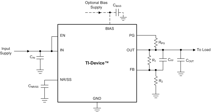
As shown in Figure 7-1, the output voltage of the TPS7A53B is set using external resistors.
 Figure 7-1 Adjustable Operation
Use Equation 4 to calculate R1 and R2. This resistive network must provide a current equal to or greater than 5μA for dc accuracy. To optimize noise and PSRR, use an R1 of 12.1kΩ.
Equation 4. VOUT = VNR/SS × (1 + R1 / R2)
Table 7-2 shows the resistor combinations required to achieve several common rails using standard 1%-tolerance resistors.
Table 7-2 Recommended Feedback-Resistor
Values(1)
| TARGETED OUTPUT
VOLTAGE (V) |
FEEDBACK RESISTOR VALUES | CALCULATED OUTPUT VOLTAGE (V) |
|
|---|---|---|---|
| R1 (kΩ) | R2 (kΩ) | ||
| 0.6 | 12.4 | 62 | 0.600 |
| 0.7 | 12.4 | 31.2 | 0.699 |
| 0.75 | 12.4 | 24.8 | 0.750 |
| 0.8 | 12.4 | 20.8 | 0.799 |
| 0.9 | 12.4 | 15.5 | 0.90 |
| 1.0 | 12.4 | 12.4 | 1.00 |
| 1.05 | 12.4 | 11.3 | 1.048 |
| 1.1 | 12.4 | 10.4 | 1.096 |
| 1.2 | 12.4 | 8.87 | 1.19 |
| 1.5 | 12.4 | 6.2 | 1.50 |
| 1.8 | 12.4 | 4.7 | 1.81 |
| 3.30 | 12.4 | 2.21 | 3.30 |
| 5.00 | 12.4 | 1.38 | 4.99 |
(1) R1 is connected from OUT to FB; R2 is connected from FB to GND.