JAJSFH9J March 2010 – March 2020 TPS7A60-Q1 , TPS7A61-Q1
PRODUCTION DATA.
- 1 特長
- 2 アプリケーション
- 3 概要
- 4 改訂履歴
- 5 Device Comparison Table
- 6 Pin Configuration and Functions
- 7 Specifications
- 8 Detailed Description
- 9 Application and Implementation
- 10Power Supply Recommendations
- 11Layout
- 12デバイスおよびドキュメントのサポート
- 13メカニカル、パッケージ、および注文情報
パッケージ・オプション
メカニカル・データ(パッケージ|ピン)
サーマルパッド・メカニカル・データ
発注情報
8.3.1 Reset Delay and Reset Output
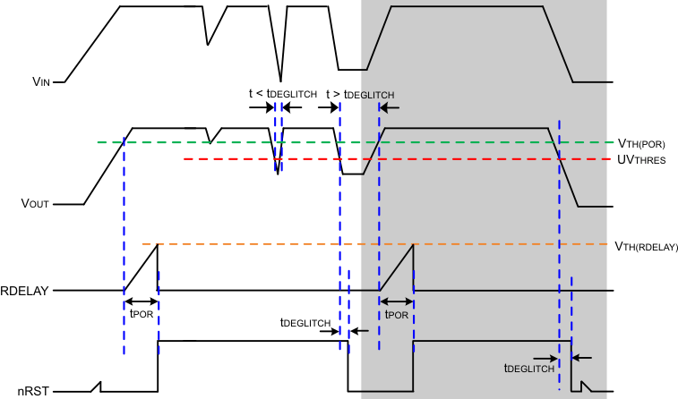
Reset delay is implemented when the device starts up to indicate that output voltage is stable and in regulation, and also when the output recovers from a negative voltage spike due to a load step or a dip in the input voltage for a specified duration. The reset-delay timer is initialized when the voltage at the output (VOUT) exceeds 93% of the regulated output voltage (3.3 V or 5 V, as applicable). The reset output (nRST) is asserted high after the power-on-reset delay (tPOR) has elapsed. If the regulated output voltage falls below 93% of the set level, nRST is asserted low after a short de-glitch time of approximately 5.5 µs (typical).
For TPS7A60-Q1 devices, the reset-delay time can be programmed by connecting an external capacitor (CDLY) to the RDELAY pin. The delay time is given by Equation 1:

where
- tPOR = reset delay time in seconds
- CDLY = reset delay capacitor value in farads, 100 pF to 100 nF
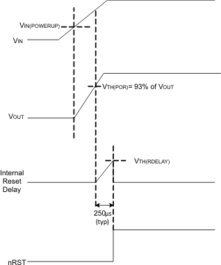
In TPS7A61xx devices, there is no RDELAY pin, and the reset-delay time is preset internally (250 µs typical).
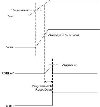
During power up, the regulator incorporates a protection scheme to limit the current through the pass element and output capacitor. When the input voltage exceeds a certain threshold (VIN(POWERUP)) level, the output voltage begins to ramp as shown in Figure 16 and Figure 17. When the output voltage reaches the power-on-reset threshold (VTH(POR)) level, a constant output current charges an external capacitor (CDLY) to an internal threshold (VTH(RDELAY)) voltage level. Then, nRST is asserted high and CDLY is discharged through an internal load. This allows CDLY to charge from approximately 0 V during the next power cycle. If no external capacitor is connected, the delay time is preset internally. This is shown in Figure 16.
In TPS7A60-Q1 devices, if the CDLY capacitor is not connected to the RDELAY pin, the reset-delay time is set internally. This is shown in Figure 17.
 Figure 16. Power Up and Reset-Delay Function With the CDLY Capacitor Connected to the RDELAY Pin for TPS7A60-Q1
  Figure 17. Power Up and Reset Delay Function With the CDLY Capacitor Not Connected or Available in TPS7A60-Q1 and TPS7A61-Q1, Respectively
 In case of negative transients in the input voltage (VIN), the reset signal is asserted low only if the output (VOUT) drops and stays below the reset threshold level (VTH(POR)) for more than the de-glitch time (tDEGLITCH). This is shown in Figure 18.
While nRST is low, if the input voltage returns to the nominal operating voltage, the normal power-up sequence is followed. nRST is asserted high, only if the output voltage exceeds the reset-threshold voltage (VTH(POR)) and the reset-delay time (tPOR) has elapsed. This is shown in the shaded region of Figure 18.
 Figure 18. Conditions for Activation of Reset