JAJSFI1E November 2010 – March 2020 TPS7A6201-Q1
PRODUCTION DATA.
- 1 特長
- 2 アプリケーション
- 3 概要
- 4 改訂履歴
- 5 Pin Configuration and Functions
- 6 Specifications
- 7 Detailed Description
- 8 Application and Implementation
- 9 Power Supply Recommendations
- 10Layout
- 11デバイスおよびドキュメントのサポート
- 12メカニカル、パッケージ、および注文情報
パッケージ・オプション
デバイスごとのパッケージ図は、PDF版データシートをご参照ください。
メカニカル・データ(パッケージ|ピン)
- KTT|5
サーマルパッド・メカニカル・データ
- KTT|5
発注情報
8.2 Typical Application
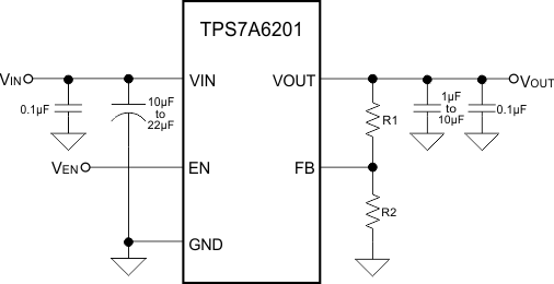
Figure 20 shows the typical application circuit for the TPS7A6201-Q1 device. Depending upon an end application, different values of external components may be used. To program the output voltage, feedback resistors (R1 and R2) must be carefully selected. Using small resistors results in higher current consumption, whereas, using very large resistors impacts the sensitivity of the regulator. Therefore, TI recommends selecting feedback resistors such that the sum of R1 and R2 is between 20 kΩ and 200 kΩ. Also, the overall tolerance of the regulated output voltage depends on the tolerance of the internal reference voltage and external feedback resistors.
A larger output capacitor may be required during fast load steps to prevent output from temporarily dropping down. TI recommends a low-ESR ceramic capacitor with a dielectric of type X5R or X7R. Additionally, a bypass capacitor can be connected at the output to decouple high-frequency noise as per the end application.
Example: If the desired regulated output voltage is 5 V, upon selecting R2, R1 can be calculated using Equation 1 (and vice versa). Knowing VREF = 1.23 V (typical), VOUT = 5 V, and selecting R2 = 20 kΩ, R1 is calculated to be 61.3 kΩ.
 Figure 20. Typical Application Schematic for TPS7A6201-Q1