JAJSFH8G June   2011  – March 2020 TPS7A63-Q1 , TPS7A6401-Q1

PRODUCTION DATA.  

  1. 特長
  2. アプリケーション
  3. 概要
    1.     Device Images
      1.      固定出力電圧オプション
      2.      可変出力電圧オプション
  4. 改訂履歴
  5. Pin Configuration and Functions
    1.     Pin Functions
  6. Specifications
    1. 6.1 Absolute Maximum Ratings
    2. 6.2 ESD Ratings
    3. 6.3 Recommended Operating Conditions
    4. 6.4 Thermal Information
    5. 6.5 Electrical Characteristics
    6. 6.6 Typical Characteristics
  7. Detailed Description
    1. 7.1 Overview
    2. 7.2 Functional Block Diagrams
    3. 7.3 Feature Description
      1. 7.3.1  Power Up, Reset Delay, and Reset Output
      2. 7.3.2  Adjustable Output Voltage
      3. 7.3.3  Chip Enable
      4. 7.3.4  Charge Pump Operation
      5. 7.3.5  Low-Power Mode
      6. 7.3.6  Undervoltage Shutdown
      7. 7.3.7  Low-Voltage Tracking
      8. 7.3.8  Integrated Fault Protection
      9. 7.3.9  Thermal Shutdown
      10. 7.3.10 Integrated Window Watchdog
        1. 7.3.10.1 Programmable-Window Watchdog
        2. 7.3.10.2 Watchdog Enable
        3. 7.3.10.3 Watchdog Service Signal
        4. 7.3.10.4 Watchdog Fault Outputs
        5. 7.3.10.5 Watchdog Initialization
        6. 7.3.10.6 Watchdog Operation
        7. 7.3.10.7 Watchdog Fault Conditions
    4. 7.4 Device Functional Modes
      1. 7.4.1 Operation With VIN Lower Than 4 V
      2. 7.4.2 Operation With VIN Larger Than 4 V
  8. Application and Implementation
    1. 8.1 Application Information
      1. 8.1.1 Example
    2. 8.2 Typical Applications
      1. 8.2.1 Typical Application Using the TPS7A6333-Q1 or TPS7A6350-Q1
        1. 8.2.1.1 Design Requirements
        2. 8.2.1.2 Detailed Design Procedure
        3. 8.2.1.3 Application Curves
      2. 8.2.2 Typical Application Using the TPS7A6401-Q1
        1. 8.2.2.1 Design Requirements
        2. 8.2.2.2 Detailed Design Procedure
        3. 8.2.2.3 Application Curves
  9. Power Supply Recommendations
  10. 10Layout
    1. 10.1 Layout Guidelines
      1. 10.1.1 Power Dissipation and Thermal Considerations
        1. 10.1.1.1 Example
    2. 10.2 Layout Example
  11. 11デバイスおよびドキュメントのサポート
    1. 11.1 関連リンク
    2. 11.2 ドキュメントの更新通知を受け取る方法
    3. 11.3 コミュニティ・リソース
    4. 11.4 商標
    5. 11.5 静電気放電に関する注意事項
    6. 11.6 Glossary
  12. 12メカニカル、パッケージ、および注文情報

パッケージ・オプション

メカニカル・データ(パッケージ|ピン)
サーマルパッド・メカニカル・データ
発注情報

Pin Configuration and Functions

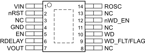
PWP Package
14-Pin HTSSOP With PowerPAD IC Package
Top View (Fixed Output Voltage Option)
TPS7A63-Q1 TPS7A6401-Q1 w_pkg_fix_lvsab1.gif
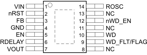
PWP Package
14-Pin HTSSOP With PowerPAD IC Package
Top View (Adjustable Output Voltage Option)
TPS7A63-Q1 TPS7A6401-Q1 pwp_pkg_adj_lvsab1.gif
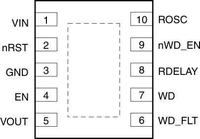
DRK Package
10-Pin VSON With Exposed Thermal Pad
Top View (Fixed Output Voltage Option)
TPS7A63-Q1 TPS7A6401-Q1 w_pkg_adj_lvsab1.gif

Pin Functions

PIN I/O DESCRIPTION
NAME PWP DRK
EN 5 4 I Chip enable pin: This is a high-voltage-tolerant input pin with an internal pulldown. A high input to this pin activates the device and turns the regulator ON. Connect this input to the VIN terminal for self-bias applications. If this pin remains unconnected, the device stays disabled.
FB 3 I Feedback pin (only applicable for TPS7A6x01-Q1): Sense voltage for error amplifier
GND 4 3 I/O Ground pin: This is signal ground pin of the device.
NC 3 Not connected (only applicable for TPS7A6333-Q1 and TPS7A6350-Q1)
NC 8 Not connected
NC 11 Not connected
NC 13 Not connected
nRST 2 2 O Reset pin: This is an open-drain reset output pin with an external pullup resistor connected to the VOUT pin.
nWD_EN 12 9 I Watchdog enable pin: A high input to this pin disables the watchdog, and vice versa. This is an active-low input pin with an internal pulldown. Leaving this pin is unconnected and floating keeps the watchdog enabled. An external microcontroller can pull this pin high momentarily to disable and reinitialize the watchdog.
RDELAY 6 8 O Reset delay timer pin: This pin programs the reset delay timer using an external capacitor (CDLY) to ground.
ROSC 14 10 O ROscillator pin: This pin programs the internal oscillator frequency (and hence the duration of the watchdog window) by connecting an external resistor to ground.
WD 10 7 I Watchdog service pin: This is an input pin to provide a service signal to the watchdog.
WD_FLAG 9 6 O Watchdog flag pin (for TPS7A6401-Q1 only): This is an active-high latched fault (that is, flag) output pin with an external pullup resistor connected to VOUT pin.
WD_FLT 9 6 O Watchdog fault pin (for TPS7A63-Q1 only): This is an active-low fault output pin with an external pullup resistor connected to the VOUT pin.
VIN 1 1 I Input voltage pin: The unregulated input voltage is supplied to this pin. A bypass capacitor connected between the VIN pin and GND pin dampens line transients on the input.
VOUT 7 5 O Regulated output voltage pin: This is a regulated voltage output (VOUT = 3.3 V or 5 V or a programmed value) pin with a limitation on maximum output current. For devices with adjustable output voltage (TPS7A6x01-Q1), connecting an external resistor network programs the output voltage. In order to achieve stable operation and prevent oscillation, connect an external output capacitor (COUT) with low ESR between this pin and GND pin.