JAJSFH8G June 2011 – March 2020 TPS7A63-Q1 , TPS7A6401-Q1
PRODUCTION DATA.
- 1 特長
- 2 アプリケーション
- 3 概要
- 4 改訂履歴
- 5 Pin Configuration and Functions
- 6 Specifications
-
7 Detailed Description
- 7.1 Overview
- 7.2 Functional Block Diagrams
- 7.3 Feature Description
- 7.4 Device Functional Modes
- 8 Application and Implementation
- 9 Power Supply Recommendations
- 10Layout
- 11デバイスおよびドキュメントのサポート
- 12メカニカル、パッケージ、および注文情報
パッケージ・オプション
メカニカル・データ(パッケージ|ピン)
- PWP|14
サーマルパッド・メカニカル・データ
- PWP|14
発注情報
7.3.10.6 Watchdog Operation
 Figure 23. Power Up, Initialization, and Normal Operation for TPS7A63-Q1
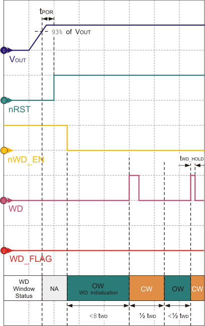
  Figure 24. Power Up, Initialization, and Normal Operation for TPS7A6401-Q1
 Figure 23 shows watchdog initialization and operation for the TPS7A63-Q1. After output voltage is in regulation and reset asserts high (clearly the chip-enable pin is high), the watchdog becomes enabled when an external signal pulls nWD_EN (the watchdog enable pin) low. This causes the watchdog to initialize and wait for a service signal during the first open window for 8× the duration of tWD. A service signal applied to the WD pin during the first open window resets the watchdog counter and a closed window starts. To prevent a fault condition from occurring, watchdog service must not occur during the closed window. Watchdog service must occur during the following open window to prevent fault condition from occurring. The fault output (WD_FLT), externally pulled up to VOUT (typically), stays high as long as the watchdog receives proper serviced and there is no fault condition.
Figure 24 shows watchdog initialization and operation for FLAG output version (TPS7A6401-Q1). The fault output (WD_FLAG), externally pulled up to VOUT (typically), stays low as long as the watchdog receives proper service and there is no fault condition.
Likewise, enabling the watchdog before powering the device on (that is, pulling the nWD_EN pin low before power up), the watchdog initializes as soon as the output voltage is in regulation and reset asserts high (see Table 2 for Conditions for Watchdog Initialization).