JAJSC95F December   2012  – December 2017 TPS7A66-Q1 , TPS7A69-Q1

PRODUCTION DATA.  

  1. 特長
  2. アプリケーション
  3. 概要
    1.     Device Images
      1.      ハードウェア・イネーブル・オプション
      2.      入力電圧センス・オプション
  4. 改訂履歴
  5. Pin Configuration and Functions
    1.     Pin Functions
  6. Specifications
    1. 6.1 Absolute Maximum Ratings
    2. 6.2 ESD Ratings
    3. 6.3 Recommended Operating Conditions
    4. 6.4 Thermal Information
    5. 6.5 Electrical Characteristics
    6. 6.6 Switching Characteristics
    7. 6.7 Typical Characteristics
  7. Detailed Description
    1. 7.1 Overview
    2. 7.2 Functional Block Diagrams
    3. 7.3 Feature Description
      1. 7.3.1 Enable (EN)
      2. 7.3.2 Regulated Output (VOUT)
      3. 7.3.3 Power-On Reset (PG)
      4. 7.3.4 Reset Delay Timer (CT)
      5. 7.3.5 Sense Comparator (SI and SO for TPS7A69-Q1)
      6. 7.3.6 Adjustable Output Voltage (FB for TPS7A6601-Q1)
      7. 7.3.7 Undervoltage Shutdown
      8. 7.3.8 Low-Voltage Tracking
      9. 7.3.9 Thermal Shutdown
    4. 7.4 Device Functional Modes
      1. 7.4.1 Regulation
      2. 7.4.2 Disabled
      3. 7.4.3 Operation With V(VinUVLO)< VIN < VIN(min)
  8. Application and Implementation
    1. 8.1 Application Information
    2. 8.2 Typical Applications
      1. 8.2.1 TPS7A66-Q1 Typical Application
        1. 8.2.1.1 Design Requirements
        2. 8.2.1.2 Detailed Design Procedure
          1. 8.2.1.2.1 Input Capacitor
          2. 8.2.1.2.2 Output Capacitor
        3. 8.2.1.3 Application Curve
      2. 8.2.2 TPS7A69-Q1 Typical Application
        1. 8.2.2.1 Design Requirements
        2. 8.2.2.2 Detailed Design Procedure
          1. 8.2.2.2.1 Low-Voltage Tracking Threshold
        3. 8.2.2.3 Application Curve
  9. Power Supply Recommendations
  10. 10Layout
    1. 10.1 Layout Guidelines
      1. 10.1.1 Package Mounting
      2. 10.1.2 Board Layout Recommendations to Improve PSRR and Noise Performance
    2. 10.2 Layout Examples
    3. 10.3 Power Dissipation and Thermal Considerations
  11. 11デバイスおよびドキュメントのサポート
    1. 11.1 関連リンク
    2. 11.2 ドキュメントの更新通知を受け取る方法
    3. 11.3 コミュニティ・リソース
    4. 11.4 商標
    5. 11.5 静電気放電に関する注意事項
    6. 11.6 Glossary
  12. 12メカニカル、パッケージ、および注文情報

パッケージ・オプション

メカニカル・データ(パッケージ|ピン)
サーマルパッド・メカニカル・データ
発注情報

Reset Delay Timer (CT)

An external capacitor on this pin sets the timer delay before the reset pin is asserted high. The constant output current charges an external capacitor until the voltage exceeds a threshold to trip an internal comparator. If this pin is open, the default delay time is 290 µs (typ). After releasing the PG pin high, the capacitor on this pin discharges, thus allowing the capacitor to charge from approximately 0.2 V for the next power-on-reset delay-timer function.

An external capacitor, CT, defines the reset-pulse delay time, t(POR), with the charge time of:

Equation 1. TPS7A66-Q1 TPS7A69-Q1 eq1_tPOR_SLVSBL0.gif

The power-on reset initializes once the output VOUT exceeds 91.6% of the programmed value. The power-on-reset delay is a function of the value set by an external capacitor on the CT pin before the releasing of the PG pin high.
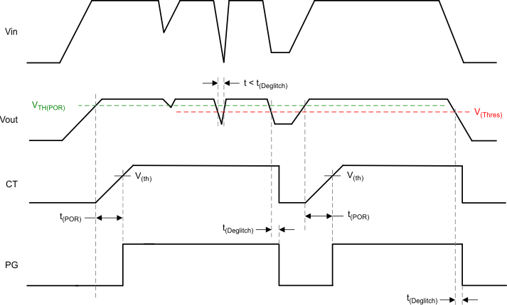
TPS7A66-Q1 TPS7A69-Q1 Cond_Act_Reset_SLVSBL0.gifFigure 21. Conditions for Activation of Reset
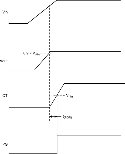
TPS7A66-Q1 TPS7A69-Q1 Ext_Prog_Reset_SLVSBL0.gifFigure 22. External Programmable Reset Delay