JAJSBS2F January 2012 – April 2017 TPS7A7001
PRODUCTION DATA.
- 1 特長
- 2 アプリケーション
- 3 概要
- 4 改訂履歴
- 5 Pin Configuration and Functions
- 6 Specifications
- 7 Detailed Description
- 8 Application and Implementation
- 9 Power Supply Recommendations
- 10Layout
- 11デバイスおよびドキュメントのサポート
- 12メカニカル、パッケージ、および注文情報
パッケージ・オプション
メカニカル・データ(パッケージ|ピン)
- DDA|8
サーマルパッド・メカニカル・データ
- DDA|8
発注情報
7 Detailed Description
7.1 Overview
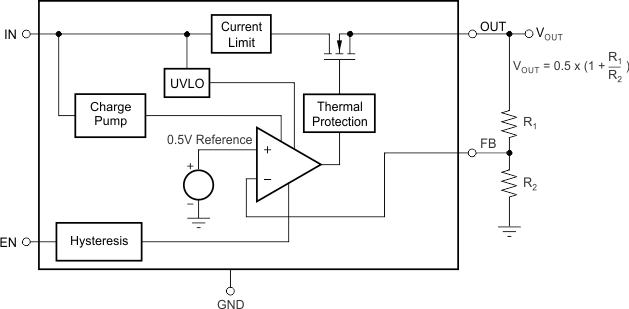
The TPS7A7001 offers a high current supply with very low dropout voltage. The TPS7A7001 is designed to minimize the required component count for a simple, small-size, and low-cost solution.
7.2 Functional Block Diagram

7.3 Feature Description
7.3.1 Enable (EN)
The enable pin (EN) is an active high logic input. When it is logic low, the device turns off and its consumption current is less than 1 µA. When it is logic high, the device turns on. The EN pin is required to be connected to a logic high or logic low level.
When the enable function is not required, connect EN to VIN.
7.3.2 Internal Current Limit
The TPS7A7001 internal current limit helps protect the regulator during fault conditions. During current limit, the output sources a fixed amount of current that is largely independent of output voltage. For reliable operation, the device should not be operated in a current limit state for extended periods of time.
Powering on the device with the enable pin, or increasing the input voltage above the minimum operating voltage while a low-impedance short exists on the output of the device, may result in a sequence of high-current pulses from the input to the output of the device. The energy consumed by the device is minimal during these events; therefore, there is no failure risk. Additional input capacitance helps to mitigate the load transient requirement of the upstream supply during these events.
7.4 Device Functional Modes
Table 1 provides a quick comparison between the normal, dropout, and disabled modes of operation.
Table 1. Device Functional Mode Comparison
| OPERATING MODE | PARAMETER | |||
|---|---|---|---|---|
| VIN | EN | IOUT | TJ | |
| Normal | VIN > VOUT(nom) + VDO | VEN > VEN(HI) | IOUT < ICL | TJ < TSD |
| Dropout | VIN < VOUT(nom) + VDO | VEN > VEN(HI) | IOUT < ICL | TJ < TSD |
| Disabled | — | VEN < VEN(LO) | — | TJ > TSD |
7.4.1 Normal Operation
The device regulates to the nominal output voltage under the following conditions:
- The input voltage is greater than the nominal output voltage plus the dropout voltage (VOUT(nom) + VDO).
- The enable voltage has previously exceeded the enable rising threshold voltage and not yet decreased below the enable falling threshold.
- The output current is less than the current limit (IOUT < ICL).
- The device junction temperature is less than the thermal shutdown temperature (TJ < TSD).
7.4.2 Dropout Operation
If the input voltage is lower than the nominal output voltage plus the specified dropout voltage, but all other conditions are met for normal operation, the device operates in dropout mode. In this mode, the output voltage tracks the input voltage. During this mode, the transient performance of the device becomes significantly degraded because the pass device is in a triode state and no longer controls the current through the LDO. Line or load transients in dropout can result in large output-voltage deviations.