JAJSBS2F January 2012 – April 2017 TPS7A7001
PRODUCTION DATA.
- 1 特長
- 2 アプリケーション
- 3 概要
- 4 改訂履歴
- 5 Pin Configuration and Functions
- 6 Specifications
- 7 Detailed Description
- 8 Application and Implementation
- 9 Power Supply Recommendations
- 10Layout
- 11デバイスおよびドキュメントのサポート
- 12メカニカル、パッケージ、および注文情報
パッケージ・オプション
メカニカル・データ(パッケージ|ピン)
- DDA|8
サーマルパッド・メカニカル・データ
- DDA|8
発注情報
8 Application and Implementation
NOTE
Information in the following applications sections is not part of the TI component specification, and TI does not warrant its accuracy or completeness. TI’s customers are responsible for determining suitability of components for their purposes. Customers should validate and test their design implementation to confirm system functionality.
8.1 Application Information
8.1.1 Input Capacitor (IN)
Although an input capacitor is not required for stability, it is recommended to connect a 1-µF to 10-µF low equivalent series resistance (ESR) capacitor across IN and GND near the device.
8.1.2 Output Capacitor (OUT)
The TPS7A7001 is stable with standard ceramic capacitors with capacitance values from 4.7 µF to 47 µF without a feedforward capacitor. For output capacitors from 47 µF to 200 µF, a feedforward capacitor of at least 220 pF must be used. The TPS7A7001 is evaluated using an X5R-type, 10-µF ceramic capacitor. X5R- and X7R-type capacitors are recommended because of minimal variation in value and ESR over temperature. Maximum ESR must be less than 1 Ω.
As with any regulator, increasing the size of the output capacitor reduces overshoot and undershoot magnitude, but increases duration of the transient response.
8.1.3 Feedback Resistors (FB)
The voltage on the FB pin sets the output voltage and is determined by the values of R1 and R2. The values of R1 and R2 can be calculated for any voltage using the formula given in Equation 1:

Table 2 shows the recommended resistor values for the best performance of the TPS7A7001. If the values in Table 2 are not used, keep the value of R2 between 27 kΩ and 33 kΩ. In Table 2, E96 series resistors are used. For the actual design, pay attention to any resistor error factors.
Table 2. Sample Resistor Values for Common Output Voltages
| VOUT | R1 | R2 |
|---|---|---|
| 1.0 V | 30.1 kΩ | 30.1 kΩ |
| 1.2 V | 42.2 kΩ | 30.1 kΩ |
| 1.5 V | 60.4 kΩ | 30.1 kΩ |
| 1.8 V | 78.7 kΩ | 30.1 kΩ |
| 2.5 V | 121 kΩ | 30.1 kΩ |
| 3.0 V | 150 kΩ | 30.1 kΩ |
| 3.3 V | 169 kΩ | 30.1 kΩ |
| 5.0 V | 274 kΩ | 30.1 kΩ |
8.2 Typical Application
 Figure 6. Typical Application
8.2.1 Design Requirements
Table 3 lists the design parameters.
Table 3. Design Parameters
| PARAMETER | DESIGN REQUIREMENT |
|---|---|
| Input voltage | 3.3 V |
| Output voltage | 2.5 V |
| Maximum output current | 1.2 A |
8.2.2 Detailed Design Procedure
Select the desired device based on the output voltage.
Provide an input supply with adequate headroom to account for dropout and output current to account for the GND terminal current, and power the load.
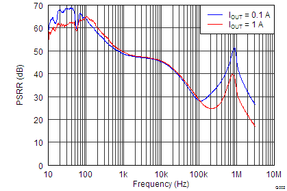
8.2.3 Application Curve

| VIN = 5.0 V, VOUT = 3.3 V |