SBVS209D May 2013 – April 2017 TPS7A7002
PRODUCTION DATA.
- 1 Features
- 2 Applications
- 3 Description
- 4 Revision History
- 5 Pin Configuration and Functions
- 6 Specifications
- 7 Detailed Description
- 8 Application and Implementation
- 9 Power Supply Recommendations
- 10Layout
- 11Device and Documentation Support
- 12Mechanical, Packaging, and Orderable Information
パッケージ・オプション
メカニカル・データ(パッケージ|ピン)
- DDA|8
サーマルパッド・メカニカル・データ
- DDA|8
発注情報
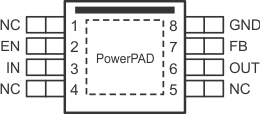
5 Pin Configuration and Functions
Pin Functions
| PIN | I/O | DESCRIPTION | |
|---|---|---|---|
| NAME | NO. | ||
| EN | 2 | I | Enable input. Pulling this pin to less than 0.5 V turns the regulator off. Connect to VIN if not being used. |
| FB | 7 | I | This pin is the output voltage feedback input through voltage dividers. See Table 2 for more details. |
| GND | 8 | — | Ground pin |
| IN | 3 | I | Input pin. Although it is not required for stability, TI recommends connecting a 1-μF to 10-μF capacitor with low equivalent series resistance (ESR) across this pin and GND. |
| NC | 1, 4, 5 | — | Not internally connected. The NC pins are not connected to any electrical node. TI recommends connecting the NC pins to large-area planes. |
| OUT | 6 | O | Regulated output pin. A 4.7-μF or larger capacitor of any type is required for stability. |
| PowerPAD | — | — | TI strongly recommends connecting the thermal pad to a large-area ground plane. If an electrically floating, dedicated thermal plane is available, the thermal pad can also be connected to it. |
