JAJSM31 May   2022 TPS7A74

ADVANCE INFORMATION  

  1. 特長
  2. アプリケーション
  3. 概要
  4. Revision History
  5. Pin Configuration and Functions
  6. Specifications
    1. 6.1 Absolute Maximum Ratings
    2. 6.2 ESD Ratings
    3. 6.3 Recommended Operating Conditions
    4. 6.4 Thermal Information
    5. 6.5 Electrical Characteristics
    6. 6.6 Typical Characteristics
  7. Detailed Description
    1. 7.1 Overview
    2. 7.2 Functional Block Diagram
    3. 7.3 Feature Description
      1. 7.3.1 Enable and Shutdown
      2. 7.3.2 Active Discharge
      3. 7.3.3 Global Undervoltage Lockout (UVLO) Circuit
      4. 7.3.4 Internal Current Limit
      5. 7.3.5 Thermal Shutdown Protection (TSD)
    4. 7.4 Device Functional Modes
      1. 7.4.1 Normal Operation
      2. 7.4.2 Dropout Operation
      3. 7.4.3 Disabled
    5. 7.5 Programming
      1. 7.5.1 Programmable Soft-Start
      2. 7.5.2 Sequencing Requirements
  8. Application and Implementation
    1. 8.1 Application Information
      1. 8.1.1 Adjusting the Output Voltage
      2. 8.1.2 Input, Output, and Bias Capacitor Requirements
      3. 8.1.3 Transient Response
      4. 8.1.4 Dropout Voltage
      5. 8.1.5 Output Noise
      6. 8.1.6 Estimating Junction Temperature
    2. 8.2 Typical Application
      1. 8.2.1 FPGA I/O Supply at 1.8 V With a Bias Rail
        1. 8.2.1.1 Design Requirements
        2. 8.2.1.2 Detailed Design Procedure
        3. 8.2.1.3 Application Curves
  9. Power Supply Recommendations
  10. 10Layout
    1. 10.1 Layout Guidelines
      1. 10.1.1 Estimating Junction Temperature
    2. 10.2 Layout Example
  11. 11Device and Documentation Support
    1. 11.1 Device Support
      1. 11.1.1 Development Support
        1. 11.1.1.1 Evaluation Modules
        2. 11.1.1.2 Spice Models
    2. 11.2 Documentation Support
      1. 11.2.1 Related Documentation
    3. 11.3 Receiving Notification of Documentation Updates
    4. 11.4 サポート・リソース
    5. 11.5 Trademarks
    6. 11.6 Electrostatic Discharge Caution
    7. 11.7 Glossary
  12. 12Mechanical, Packaging, and Orderable Information

パッケージ・オプション

メカニカル・データ(パッケージ|ピン)
サーマルパッド・メカニカル・データ
発注情報

Estimating Junction Temperature

Using the thermal metrics ΨJT and ΨJB, as shown in the Section 6.4 table, the junction temperature can be estimated with corresponding formulas (given in Equation 11). For backwards compatibility, an older θJC(top) parameter is listed as well.

Equation 11. GUID-18FA9619-2DB8-4E71-BFEF-08352B6380E6-low.gif

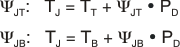
Where PD is the power dissipation shown by Equation 9, TT is the temperature at the center-top of the package, and TB is the PCB temperature measured 1 mm away from the package on the PCB surface.

Note: Both TT and TB can be measured on actual application boards using a thermo-gun (an infrared thermometer).

For more information about measuring TT and TB, see the Using New Thermal Metrics application note, available for download at www.ti.com.

For a more detailed discussion of why TI does not recommend using θJC(top) to determine thermal characteristics, see the Using New Thermal Metrics application report, available for download at www.ti.com. For further information, see the IC Package Thermal Metrics application report, also available on the TI website.