JAJSH18A March 2019 – September 2019 TPS7A78
PRODUCTION DATA.
- 1 特長
- 2 アプリケーション
- 3 概要
- 4 改訂履歴
- 5 概要(続き)
- 6 Pin Configuration and Functions
- 7 Specifications
-
8 Detailed Description
- 8.1 Overview
- 8.2 Functional Block Diagram
- 8.3
Feature Description
- 8.3.1 Active Bridge Control
- 8.3.2 Full-Bridge (FB) and Half-Bridge (HB) Configurations
- 8.3.3 4:1 Switched-Capacitor Voltage Reduction
- 8.3.4 Undervoltage Lockout Circuits (VUVLO_SCIN) and (VUVLO_LDO_IN)
- 8.3.5 Dropout Voltage Regulation
- 8.3.6 Current Limit
- 8.3.7 Programmable Power-Fail Detection
- 8.3.8 Power-Good (PG) Detection
- 8.3.9 Thermal Shutdown
- 8.4 Device Functional Modes
-
9 Application and Implementation
- 9.1
Application Information
- 9.1.1 Recommended Capacitor Types
- 9.1.2 Input and Output Capacitors Requirements
- 9.1.3 Startup Behavior
- 9.1.4 Load Transient
- 9.1.5 Standby Power and Output Efficiency
- 9.1.6 Reverse Current
- 9.1.7 Switched-Capacitor Stage Output Impedance
- 9.1.8 Power Dissipation (PD)
- 9.1.9 Estimating Junction Temperature
- 9.2
Typical Application
- 9.2.1 Design Requirements
- 9.2.2
Detailed Design Procedure
- 9.2.2.1 Calculating the Cap-Drop Capacitor CS
- 9.2.2.2 Calculating the Surge Resistor RS
- 9.2.2.3 Checking for the Device Maximum ISHUNT Current
- 9.2.2.4 Calculating the Bulk Capacitor CSCIN
- 9.2.2.5 Calculating the PFD Pin Resistor Dividers for a Power-Fail Detection
- 9.2.2.6 Summary of the Typical Application Design Components
- 9.2.3 Application Curves
- 9.1
Application Information
- 10Power Supply Recommendations
- 11Layout
- 12デバイスおよびドキュメントのサポート
- 13メカニカル、パッケージ、および注文情報
パッケージ・オプション
メカニカル・データ(パッケージ|ピン)
- PWP|14
サーマルパッド・メカニカル・データ
- PWP|14
発注情報
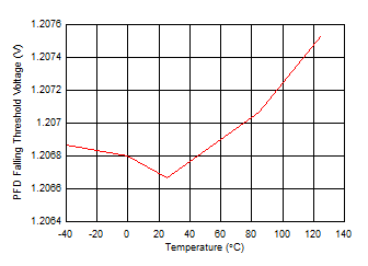
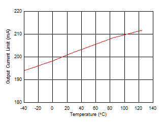
7.7 Typical Characteristics
at operating temperature TJ = 25°C, VAC supply = 120 VRMS per 60 Hz, full-bridge (FB) bridge configuration, CS = 1.0 µF, CSCIN = 220 µF, CSC1 = 1.0 µF, CSC2 = 2.2 µF, CLDO_IN = 10 µF, CLDO_OUT = 1.0 µF, and IOUT = 1 mA (unless otherwise noted)
| VAC = 70 VRMS to 270 VRMS, VLDO_OUT = 5.0 V |

| VSCIN = 17 V, VLDO_OUT ≤ 3.4 V |

| VSCIN = 17 V, VLDO_OUT = 3.3 V |


| FB configuration, scope bandwidth = 10 MHz,
IOUT = 1 mA |

| CS = 2.2 µF, CSCIN = 22 µF, CLDO_IN = 1.0 µF, IOUT = 10 mA |

| VSCIN = 19 V, VLDO_OUT ≤ 3.4 V |

| VLDO_OUT = 5.0 V, IOUT = 0 mA to 120 mA |

| VSCIN = 19 V, VLDO_OUT ≤ 3.4 V |

| VSCIN = 19 V, VLDO_OUT = 3.3 V |


| FB configuration, scope bandwidth = 10 MHz,
IOUT = 120 mA |

| CS = 100 nF, CSCIN = 22 µF, CLDO_IN = 1.0 µF, IOUT = 10 mA |