JAJSH18A March 2019 – September 2019 TPS7A78
PRODUCTION DATA.
- 1 特長
- 2 アプリケーション
- 3 概要
- 4 改訂履歴
- 5 概要(続き)
- 6 Pin Configuration and Functions
- 7 Specifications
-
8 Detailed Description
- 8.1 Overview
- 8.2 Functional Block Diagram
- 8.3
Feature Description
- 8.3.1 Active Bridge Control
- 8.3.2 Full-Bridge (FB) and Half-Bridge (HB) Configurations
- 8.3.3 4:1 Switched-Capacitor Voltage Reduction
- 8.3.4 Undervoltage Lockout Circuits (VUVLO_SCIN) and (VUVLO_LDO_IN)
- 8.3.5 Dropout Voltage Regulation
- 8.3.6 Current Limit
- 8.3.7 Programmable Power-Fail Detection
- 8.3.8 Power-Good (PG) Detection
- 8.3.9 Thermal Shutdown
- 8.4 Device Functional Modes
-
9 Application and Implementation
- 9.1
Application Information
- 9.1.1 Recommended Capacitor Types
- 9.1.2 Input and Output Capacitors Requirements
- 9.1.3 Startup Behavior
- 9.1.4 Load Transient
- 9.1.5 Standby Power and Output Efficiency
- 9.1.6 Reverse Current
- 9.1.7 Switched-Capacitor Stage Output Impedance
- 9.1.8 Power Dissipation (PD)
- 9.1.9 Estimating Junction Temperature
- 9.2
Typical Application
- 9.2.1 Design Requirements
- 9.2.2
Detailed Design Procedure
- 9.2.2.1 Calculating the Cap-Drop Capacitor CS
- 9.2.2.2 Calculating the Surge Resistor RS
- 9.2.2.3 Checking for the Device Maximum ISHUNT Current
- 9.2.2.4 Calculating the Bulk Capacitor CSCIN
- 9.2.2.5 Calculating the PFD Pin Resistor Dividers for a Power-Fail Detection
- 9.2.2.6 Summary of the Typical Application Design Components
- 9.2.3 Application Curves
- 9.1
Application Information
- 10Power Supply Recommendations
- 11Layout
- 12デバイスおよびドキュメントのサポート
- 13メカニカル、パッケージ、および注文情報
パッケージ・オプション
メカニカル・データ(パッケージ|ピン)
- PWP|14
サーマルパッド・メカニカル・データ
- PWP|14
発注情報
9.1.6 Reverse Current
Excessive reverse current can damage the TPS7A78. Reverse current flows through the intrinsic body diode of the pass-transistor instead of the normal conducting channel. At high magnitudes, this current flow degrades the long-term reliability of the device.
Conditions where reverse current can occur are:
- If the device has a large CLDO_OUT and the input supply collapses with little or no load current
- The LDO_OUT pin is biased when the input supply is not present
- The LDO_OUT pin is biased above the voltage of the LDO_IN pin
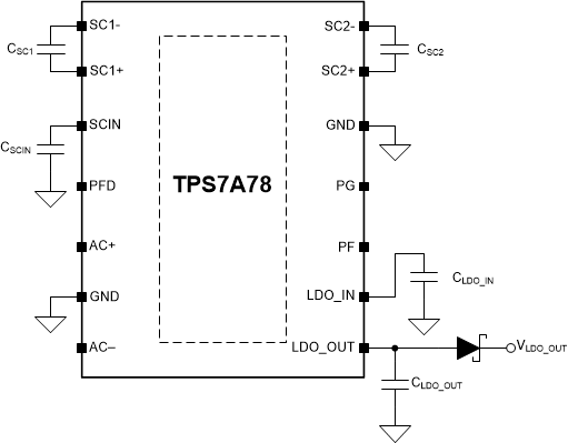
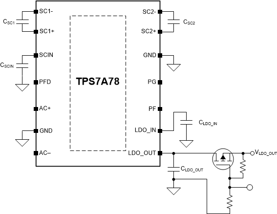
If reverse current flow is expected in the application, external protection is recommended to provide protect. Reverse current is not limited within the device, so external limiting is required, as illustrated in Figure 30 and Figure 31, if extended reverse-voltage operation is anticipated.
 Figure 30. Example Circuit for Reverse Current Protection Using a Schottky Diode
  Figure 31. Example Circuit for Reverse Current Protection Using a P-Channel FET