JAJSDB7B June 2017 – October 2021 TPS7A83A
PRODUCTION DATA
- 1 特長
- 2 アプリケーション
- 3 概要
- 4 Revision History
- 5 概要 (続き)
- 6 Pin Configuration and Functions
-
7 Specifications
- 7.1 Absolute Maximum Ratings
- 7.2 ESD Ratings
- 7.3 Recommended Operating Conditions
- 7.4 Thermal Information
- 7.5 Electrical Characteristics: General
- 7.6 Electrical Characteristics: TPS7A8300A
- 7.7 Electrical Characteristics: TPS7A8301A
- 7.8 Typical Characteristics: TPS7A8300A
- 7.9 Typical Characteristics: TPS7A8301A
- 8 Detailed Description
-
9 Application and Implementation
- 9.1
Application Information
- 9.1.1
External Component Selection
- 9.1.1.1 Adjustable Operation
- 9.1.1.2 ANY-OUT Programmable Output Voltage
- 9.1.1.3 ANY-OUT Operation
- 9.1.1.4 Increasing ANY-OUT Resolution for LILO Conditions
- 9.1.1.5 Recommended Capacitor Types
- 9.1.1.6 Input and Output Capacitor Requirements (CIN and COUT)
- 9.1.1.7 Feed-Forward Capacitor (CFF)
- 9.1.1.8 Noise-Reduction and Soft-Start Capacitor (CNR/SS)
- 9.1.2 Start Up
- 9.1.3 AC and Transient Performance
- 9.1.4 DC Performance
- 9.1.5 Sequencing Requirements
- 9.1.6 Negatively Biased Output
- 9.1.7 Reverse Current
- 9.1.8 Power Dissipation (PD)
- 9.1.1
External Component Selection
- 9.2 Typical Application
- 9.1
Application Information
- 10Power Supply Recommendations
- 11Layout
- 12Device and Documentation Support
- 13Mechanical, Packaging, and Orderable Information
パッケージ・オプション
メカニカル・データ(パッケージ|ピン)
サーマルパッド・メカニカル・データ
発注情報
9.1.3.1 Power-Supply Rejection Ratio (PSRR)
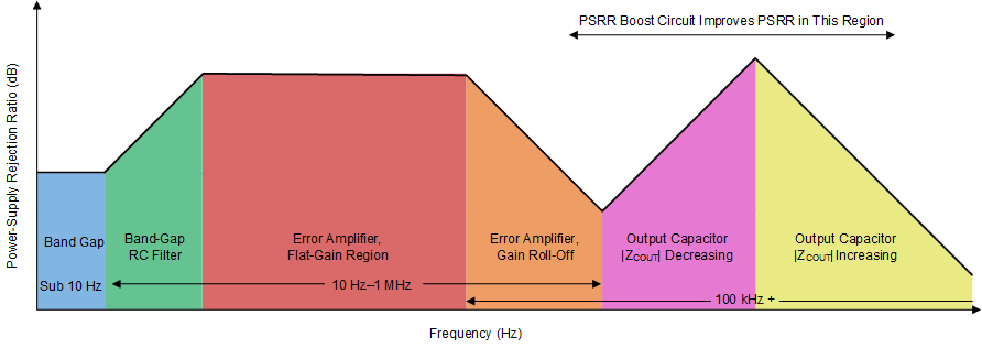
PSRR is a measure of how well the LDO control loop rejects signals from VIN to VOUT across the frequency spectrum (usually 10 Hz to 10 MHz). Equation 9 gives the PSRR calculation as a function of frequency for the input signal [VIN(f)] and output signal [VOUT(f)].

Even though PSRR is a loss in signal amplitude, PSRR is shown as positive values in decibels (dB) for convenience.
Figure 9-6 shows a simplified diagram of PSRR versus frequency.
 Figure 9-6 Power-Supply Rejection Ratio Diagram
An LDO is often employed not only as a dc/dc regulator, but also to provide exceptionally clean power-supply voltages that exhibit ultra-low noise and ripple to sensitive system components. This usage is especially true for the TPS7A83A.
The TPS7A83A features an innovative circuit to boost the PSRR from 200 kHz to 1 MHz; see Figure 7-1. To achieve the maximum benefit of this PSRR boost circuit, use a capacitor with a minimum impedance in the 100-kHz to 1-MHz band.