SBVS281A March 2016 – July 2016 TPS7A87
PRODUCTION DATA.
- 1 Features
- 2 Applications
- 3 Description
- 4 Revision History
- 5 Pin Configuration and Functions
- 6 Specifications
- 7 Detailed Description
- 8 Application and Implementation
- 9 Power Supply Recommendations
- 10Layout
- 11Device and Documentation Support
- 12Mechanical, Packaging, and Orderable Information
パッケージ・オプション
デバイスごとのパッケージ図は、PDF版データシートをご参照ください。
メカニカル・データ(パッケージ|ピン)
- RTJ|20
サーマルパッド・メカニカル・データ
- RTJ|20
発注情報
7 Detailed Description
7.1 Overview
The TPS7A87 is a monolithic, dual-channel, low-dropout (LDO) regulator, and each channel is low-noise, high-PSRR, and capable of sourcing a 500-mA load with only 100 mV of maximum dropout. These features make the device a robust solution to solve many challenging problems in generating a clean, accurate power supply.
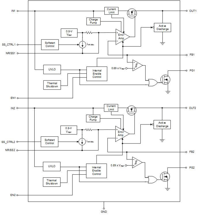
The various features for each of the TPS7A87 fully independent LDOs simplify using the device in a variety of applications. As detailed in the Functional Block Diagram section, these features are organized into three categories, as shown in Table 1.
Table 1. Features
| VOLTAGE REGULATION | SYSTEM START-UP | INTERNAL PROTECTION |
|---|---|---|
| High accuracy | Programmable soft-start | Foldback current limit |
| Low-noise, high-PSRR output | Sequencing controls | Thermal shutdown |
| Fast transient response | Power-good output |
7.2 Functional Block Diagram

NOINDENT:
7.3 Feature Description
7.3.1 Voltage Regulation Features
7.3.1.1 DC Regulation
An LDO functions as a class-B amplifier in which the input signal is the internal reference voltage (VREF), as shown in Figure 41. VREF is designed to have a very low-bandwidth at the input to the error amplifier through the use of a low-pass filter (VNR/SSx).
As such, the reference can be considered as a pure dc input signal. The low output impedance of an LDO comes from the combination of the output capacitor and pass element. The pass element also presents a high input impedance to the source voltage when operating as a current source. A positive LDO can only source current because of the class-B architecture.
This device achieves a maximum of 1% output voltage accuracy primarily because of the high-precision band-gap voltage (VBG) that creates VREF. The low dropout voltage (VDO) reduces the thermal power dissipation required by the device to regulate the output voltage at a given current level, thereby improving system efficiency. Combined, these features help make this device a good approximation of an ideal voltage source.
This device replaces two stand-alone power-supplies, and also provides load-to-load isolation. The LDOs can also be put in series (cascaded) to achieve even higher PSRR by connecting the output of one channel to the input of the other channel.

NOTE:
VOUTx = VREF × (1 + R1x / R2x).7.3.1.2 AC and Transient Response
Each LDO responds quickly to a transient (large-signal response) on the input supply (line transient) or the output current (load transient) resulting from the LDO high-input impedance and low output-impedance across frequency. This same capability also means that each LDO has a high power-supply rejection-ratio (PSRR) and, when coupled with a low internal noise-floor (Vn), the LDO approximates an ideal power supply in ac (small-signal) and large-signal conditions.
The performance and internal layout of the device minimizes the coupling of noise from one channel to the other channel (crosstalk). Good printed circuit board (PCB) layout minimizes the crosstalk.
The choice of external component values optimizes the small- and large-signal response. The NR/SSx capacitor (CNR/SSx) and feed-forward capacitor (CFFx) easily reduce the device noise floor and improve PSRR; see the Optimizing Noise and PSRR section for more information on optimizing the noise and PSRR performance.
7.3.2 System Start-Up Features
In many different applications, the power-supply output must turn-on within a specific window of time to either ensure proper operation of the load or to minimize the loading on the input supply or other sequencing requirements. Each LDO start-up is well-controlled and user-adjustable, solving the demanding requirements faced by many power-supply design engineers in a simple fashion.
7.3.2.1 Programmable Soft-Start (NR/SSx)
Soft-start directly controls the output start-up time and indirectly controls the output current during start-up (in-rush current).
The external capacitor at the NR/SSx pin (CNR/SSx) sets the output start-up time by setting the rise time of the internal reference (VNR/SSx), as shown in Figure 42. SS_CTRLx provides additional control over the rise time of the internal reference by enabling control over the charging current (INR/SSx) for CNR/SSx. The voltage at the SS_CTRLx pin (VSS_CTRLx) must be connected to ground (GND) or VINx.
Note that if CNR/SSx = 0 nF and the SS_CTRLx pin is connected to VINx, then the output voltage overshoots during start-up.
 Figure 42. Simplified Soft-Start Circuit
7.3.2.2 Sequencing
Controlling when a single power supply turns on can be difficult in a power distribution network (PDN) because of the high power levels inherent in a PDN, and the variations between all of the supplies. Control of each channel turn-on and turn-off time is set by the specific channel enable circuit (ENx) and undervoltage lockout circuit (UVLOx), as shown in Figure 43 and Table 2.
 Figure 43. Simplified Turn-On Control
Table 2. Sequencing Functionality Table
| INPUT VOLTAGE | ENABLE STATUS | LDO STATUS | ACTIVE DISCHARGE | POWER-GOOD |
|---|---|---|---|---|
| VINx ≥ VUVLOx | ENx = 1 | On | Off | PGx = 1 when VOUTx ≥ VIT(PGx) |
| ENx = 0 | Off | On | PGx = 0 | |
| VINx < VUVLOx – VHYS | ENx = don't care | Off | On(1) | PGx = 0 |
7.3.2.2.1 Enable (ENx)
The enable signal (VENx) is an active-high digital control that enables the LDO when the enable voltage is past the rising threshold (VENx ≥ VIH(ENx)) and disables the LDO when the enable voltage is below the falling threshold (VENx ≤ VIL(ENx)). The exact enable threshold is between VIH(ENx) and VIL(ENx) because ENx is a digital control. In applications that do not use the enable control, connect ENx to VINx.
7.3.2.2.2 Undervoltage Lockout (UVLOx) Control
The UVLOx circuit responds quickly to glitches on VINx and attempts to disable the output of the device if either of these rails collapse.
As a result of the fast response time of the input supply UVLOx circuit, fast and short line transients well below the input supply UVLOx falling threshold (brownouts) can cause momentary glitches during the edges of the transient. These glitches are typical in most LDOs and, in most applications, the brownouts required for these glitches do not result from the local input capacitance; see the Undervoltage Lockout (UVLOx) Control section for more details.
7.3.2.2.3 Active Discharge
When either ENx or UVLOx is low, the device connects a resistor of several hundred ohms from VOUTx to GND, discharging the output capacitance.
Do not rely on the active discharge circuit for discharging large output capacitors when the input voltage drops below the targeted output voltage. Current flows from the output to the input (reverse current) when VOUTx > VINx, which can cause damage to the device (when VOUTx > VINx + 0.3 V); see the Reverse Current Protection section for more details.
7.3.2.3 Power-Good Output (PGx)
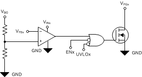
The PGx signal provides an easy solution to meet demanding sequencing requirements because PGx signals when the output nears its nominal value. PGx can be used to signal other devices in a system when the output voltage is near, at, or above the set output voltage (VOUTx(Target)). A simplified schematic is shown in Figure 44.
The PGx signal is an open-drain digital output that requires a pullup resistor to a voltage source and is active high. The power-good circuit sets the PGx pin into a high-impedance state to indicate that the power is good.
Using a large feed-forward capacitor (CFFx) delays the output voltage and, because the power-good circuit monitors the FBx pin, the PGx signal can indicate a false positive. A simple solution to this scenario is to use an external voltage detector device, such as the TPS3780; see the Feed-Forward Capacitor (CFFx) section for more information.
 Figure 44. Simplified PGx Circuit
7.3.3 Internal Protection Features
In many applications, fault events can occur that damage devices in the system. Short-circuits and excessive heat are the most common fault events for power supplies. The TPS7A87 implements circuitry for each LDO to protect the device and its load during these events. Continuously operating in these fault conditions or above a junction temperature of 125°C is not recommended because the long-term reliability of the device is reduced.
7.3.3.1 Foldback Current Limit (ICLx)
The internal current limit circuit protects the LDO against short-circuit and excessive load current conditions. The output current decreases (folds back) when the output voltage falls to better protect the device, as described in Figure 19. Each channel features its own independent current limit circuit.
7.3.3.2 Thermal Protection (Tsdx)
The thermal shutdown circuit protects the LDO against excessive heat in the system, either resulting from current limit or high ambient temperature. Each channel features its own independent thermal shutdown circuit.
The output of the LDO turns off when the LDO temperature (junction temperature, TJ) exceeds the rising thermal shutdown temperature (Tsdx). The output turns on again after TJ decreases below the falling thermal shutdown temperature (Tsdx).
A high power dissipation across the device, combined with a high ambient temperature (TA), can cause TJ to be greater than or equal to Tsdx, triggering the thermal shutdown and causing the output to fall to 0 V. The LDO can cycle on and off when thermal shutdown is reached under these conditions.
7.4 Device Functional Modes
Table 3 provides a quick comparison between the regulation and disabled operation.
Table 3. Device Functional Modes Comparison
| OPERATING MODE | PARAMETER | |||
|---|---|---|---|---|
| VINx | ENx | IOUTx | TJ | |
| Regulation(1) | VINx > VOUTx(nom) + VDO | VENx > VIH(ENx) | IOUTx < ICLx | TJ < Tsd |
| Disabled(2) | VINx < VUVLOx | VENx < VIL(ENx) | — | TJ > Tsd |
7.4.1 Regulation
The device regulates the output to the targeted output voltage when all the conditions in Table 3 are met.
7.4.2 Disabled
When disabled, the pass device is turned off, the internal circuits are shutdown, and the output voltage is actively discharged to ground by an internal resistor from the output to ground.