JAJSM29A april 2023 – july 2023 TPS7A96
PRODUCTION DATA
- 1
- 1 特長
- 2 アプリケーション
- 3 概要
- 4 Revision History
- 5 Pin Configuration and Functions
- 6 Specifications
-
7 Detailed Description
- 7.1 Overview
- 7.2 Functional Block Diagram
- 7.3
Feature Description
- 7.3.1 Output Voltage Setting and Regulation
- 7.3.2 Ultra-Low Noise and Ultra-High Power-Supply Rejection Ratio (PSRR)
- 7.3.3 Programmable Current Limit and Power-Good Threshold
- 7.3.4 Programmable Soft-Start (NR/SS Pin)
- 7.3.5 Precision Enable and UVLOs
- 7.3.6 Active Discharge
- 7.3.7 Thermal Shutdown Protection (TSD)
- 7.4 Device Functional Modes
-
8 Application and Implementation
- 8.1
Application Information
- 8.1.1 Output Voltage Restart (Overshoot Prevention Circuit)
- 8.1.2 Precision Enable (External UVLO)
- 8.1.3 Undervoltage Lockout (UVLO) Operation
- 8.1.4 Dropout Voltage (VDO)
- 8.1.5 Power-Good Feedback (FB_PG Pin) and Power-Good Threshold (PG Pin)
- 8.1.6 Adjusting the Factory-Programmed Current Limit
- 8.1.7 Programmable Soft-Start and Noise-Reduction (NR/SS Pin)
- 8.1.8 Inrush Current
- 8.1.9 Optimizing Noise and PSRR
- 8.1.10 Adjustable Operation
- 8.1.11 Paralleling for Higher Output Current and Lower Noise
- 8.1.12 Recommended Capacitor Types
- 8.1.13 Load Transient Response
- 8.1.14 Power Dissipation (PD)
- 8.1.15 Estimating Junction Temperature
- 8.1.16 TPS7A96EVM-106 Thermal Analysis
- 8.2 Typical Application
- 8.3 Power Supply Recommendations
- 8.4 Layout
- 8.1
Application Information
- 9 Device and Documentation Support
- 10Mechanical, Packaging, and Orderable Information
パッケージ・オプション
メカニカル・データ(パッケージ|ピン)
- DSC|10
サーマルパッド・メカニカル・データ
- DSC|10
発注情報
8.1.5 Power-Good Feedback (FB_PG Pin) and Power-Good Threshold (PG Pin)
For proper device operation, the resistor divider network input to the FB_PG pin must be connected. The FB_PG pin must not be left floating because this pin represents an analog input to the device internal logic and the input impedance is sampled during device start up.
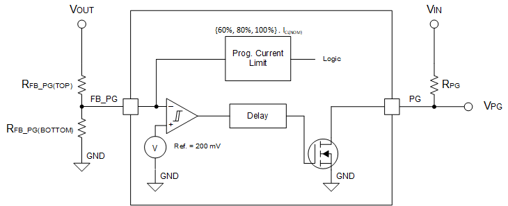
The PG pin is an output indicating whether the LDO is ready to provide power. This pin is implemented using an open-drain architecture. The FB_PG pin programs the PG pin and serves a dual purpose of programming the PG threshold assert voltage and adjusting the current limit, ICL.
The PG pin must use the minimum value or larger pullup resistor from PG to IN, as shown in Figure 8-8, or the external rail as listed in the Electrical CharacteristicsElectrical CharacteristicsElectrical CharacteristicsElectrical CharacteristicsElectrical CharacteristicsElectrical CharacteristicsElectrical Characteristics table. If PG functionality is not used, leave this pin floating or connected to GND.
The FB_PG pin uses the parallel impedance formed by the resistor divider RFB_PG(TOP) and RFB_PG(BOTTOM) to program the current limit value during LDO initialization. If this impedance is less than 12.5 kΩ, then the nominal factory-programmed, current-limit value is selected. If the input impedance is less than 50 kΩ, but greater than 12.5 kΩ, then 80% of the nominal factory-programmed current limit is selected. If the input impedance is less than 100 kΩ, but greater than 50 kΩ, then 60% of the nominal factory-programmed current limit is selected. Connect the RFB_PG(TOP) and RFB_PG(BOTTOM) resistors as indicated in this section for proper operation of the LDO. Do not float this pin.
When initialization is complete, the voltage divider provides the necessary feedback to the PG pin by setting the PG assert threshold voltage.
To properly select the values of the RFB_PG(TOP) and RFB_PG(BOTTOM) resistors, see the Adjusting the Factory-Programmed Current LimitAdjusting the Factory-Programmed Current LimitAdjusting the Factory-Programmed Current Limit section for detailed explanation and calculation.
If the current limit is set for 100% of the nominal factory-programmed current limit, the PG threshold range is not limited. A PG threshold greater than 80% is common for systems where start-up inrush current must be minimized. Lower PG thresholds can be needed in systems with fast start-up time constraints.
Setting the PG threshold based off the VFB_PG voltage sets the PG to assert when the output voltage reaches the corresponding percentage level of VFB_PG because VFB_PG is a scaled version of the output voltage.
Figure 8-8 shows the internal circuitry for both the FB_PG and PG pins.
 Figure 8-8 Programmable Power-Good
Threshold Simplified Schematic
Figure 8-8 Programmable Power-Good
Threshold Simplified SchematicThe PG pin pullup resistor value must be between 10 kΩ and 100 kΩ. The lower limit of 10 kΩ results from the maximum pulldown strength of the power-good transistor, and the upper limit of 100 kΩ results from the maximum leakage current at the power-good node. If the pullup resistor is outside of this range, then the power-good signal can possibly not read a valid digital logic level.
The state of the PG signal is only valid when the FB_PG pin resistor divider network is set properly and the device is in normal operating mode.