JAJSM29A april 2023 – july 2023 TPS7A96
PRODUCTION DATA
- 1
- 1 特長
- 2 アプリケーション
- 3 概要
- 4 Revision History
- 5 Pin Configuration and Functions
- 6 Specifications
-
7 Detailed Description
- 7.1 Overview
- 7.2 Functional Block Diagram
- 7.3
Feature Description
- 7.3.1 Output Voltage Setting and Regulation
- 7.3.2 Ultra-Low Noise and Ultra-High Power-Supply Rejection Ratio (PSRR)
- 7.3.3 Programmable Current Limit and Power-Good Threshold
- 7.3.4 Programmable Soft-Start (NR/SS Pin)
- 7.3.5 Precision Enable and UVLOs
- 7.3.6 Active Discharge
- 7.3.7 Thermal Shutdown Protection (TSD)
- 7.4 Device Functional Modes
-
8 Application and Implementation
- 8.1
Application Information
- 8.1.1 Output Voltage Restart (Overshoot Prevention Circuit)
- 8.1.2 Precision Enable (External UVLO)
- 8.1.3 Undervoltage Lockout (UVLO) Operation
- 8.1.4 Dropout Voltage (VDO)
- 8.1.5 Power-Good Feedback (FB_PG Pin) and Power-Good Threshold (PG Pin)
- 8.1.6 Adjusting the Factory-Programmed Current Limit
- 8.1.7 Programmable Soft-Start and Noise-Reduction (NR/SS Pin)
- 8.1.8 Inrush Current
- 8.1.9 Optimizing Noise and PSRR
- 8.1.10 Adjustable Operation
- 8.1.11 Paralleling for Higher Output Current and Lower Noise
- 8.1.12 Recommended Capacitor Types
- 8.1.13 Load Transient Response
- 8.1.14 Power Dissipation (PD)
- 8.1.15 Estimating Junction Temperature
- 8.1.16 TPS7A96EVM-106 Thermal Analysis
- 8.2 Typical Application
- 8.3 Power Supply Recommendations
- 8.4 Layout
- 8.1
Application Information
- 9 Device and Documentation Support
- 10Mechanical, Packaging, and Orderable Information
パッケージ・オプション
メカニカル・データ(パッケージ|ピン)
- DSC|10
サーマルパッド・メカニカル・データ
- DSC|10
発注情報
8.1.7 Programmable Soft-Start and Noise-Reduction (NR/SS Pin)
The NR/SS pin is the input to the inverting terminal of the error amplifier, see the Functional Block Diagram. A resistor connected from this pin to GND sets the output voltage by the pin internal reference current INR/SS, as given in the following equation:
Connecting a capacitor from this pin to GND significantly reduces the output noise, limits the input inrush-current, and soft-starts the output voltage. Use the minimum value or larger capacitor from NR/SS to ground as listed in the Electrical CharacteristicsElectrical CharacteristicsElectrical CharacteristicsElectrical CharacteristicsElectrical CharacteristicsElectrical CharacteristicsElectrical Characteristics table and place the NR/SS capacitor as close to the NR/SS and GND pins of the device as possible.
The device features a programmable, monotonic, voltage-controlled, soft-start circuit that is set to work with an external capacitor (CNR/SS). In addition to the soft-start feature, the CNR/SS capacitor also lowers the output voltage noise of the LDO. The soft-start feature can be used to eliminate power-up initialization problems. The controlled output voltage ramp also reduces peak inrush current during start-up, minimizing start-up transients to the input power bus.
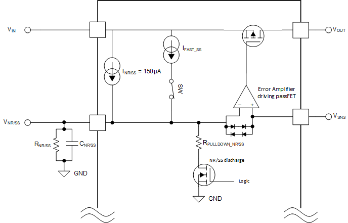
To achieve a monotonic start-up, the device output voltage tracks the VNR/SS reference voltage until this reference reaches the set value (the set output voltage). The VNR/SS reference voltage is set by the RNR/SS resistor and, during start-up, using a fast charging current (IFAST_SS) in addition to the INR/SS current, as illustrated in Figure 8-10, to charge the CNR/SS capacitor.
 Figure 8-10 Simplified Soft-Start Circuit
The 2.1-mA (typical) IFAST_SS current and 150-μA (typical) INR/SS current quickly charge CNR/SS until the voltage reaches approximately 93% of the set output voltage, then the IFAST_SS current disengages and only the INR/SS current continues to charge CNR/SS to the set output voltage level. If there is any error during start-up or the output overshoot prevention circuit is triggered, the NR/SS discharge FET turns on, thus discharging the CNR/SS capacitor to protect both the LDO and the load.
The soft-start ramp time depends on the fast start-up (IFAST_SS) charging current, the reference current (INR/SS), CNR/SS capacitor value, and the set (targeted) output voltage (VOUT(target)). Equation 4 calculates the soft-start ramp time.
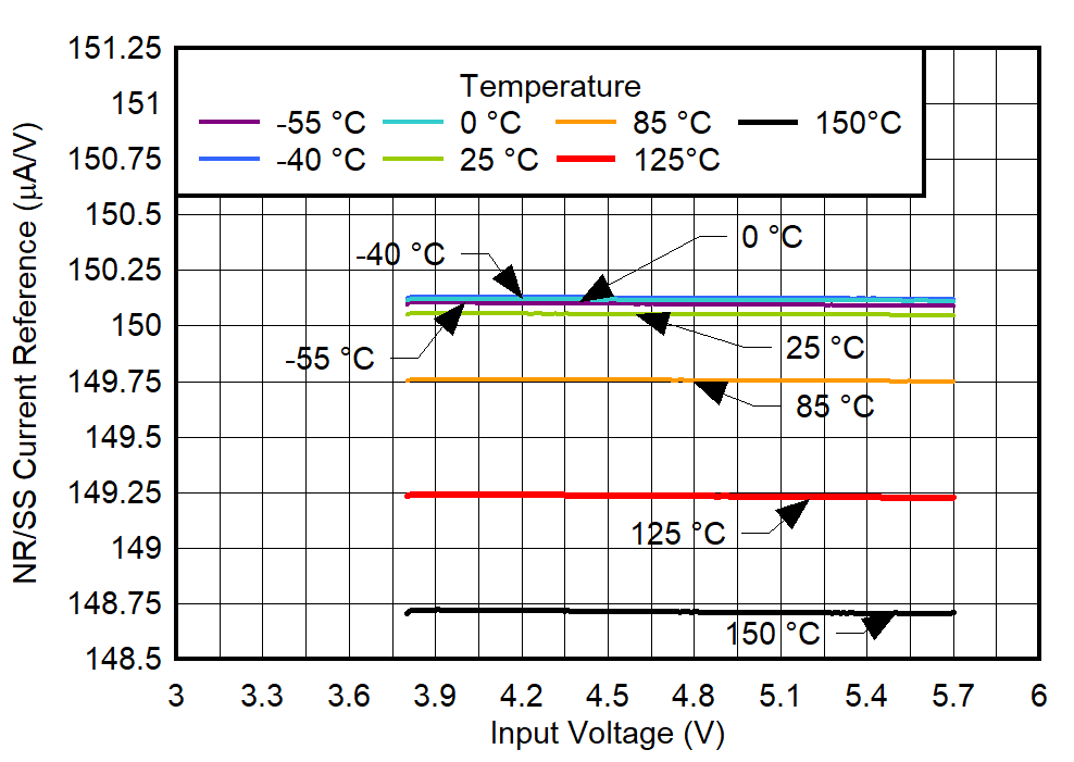
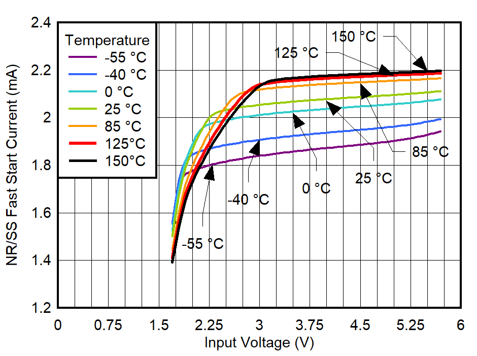
The INR/SS current is provided in the Electrical CharacteristicsElectrical CharacteristicsElectrical CharacteristicsElectrical CharacteristicsElectrical CharacteristicsElectrical CharacteristicsElectrical Characteristics table and has a value of 150 μA (typical). The IFAST_SS current has a value of 2 mA (typical) for VIN > 2.5 V. Figure 8-11 and Figure 8-12 show the INR/SS and IFAST_SS current versus VIN and temperature.
 Figure 8-11 INR/SS Reference vs Input
Voltage and Temperature for VOUT = 3.3 V
 Figure 8-12 IFAST_SS Reference vs
Input Voltage and Temperature for VOUT = 3.3 V
Figure 8-12 IFAST_SS Reference vs
Input Voltage and Temperature for VOUT = 3.3 VBecause the error amplifier is always operating in unity-gain configuration, the output voltage noise can only be adjusted by increasing the CNR/SS capacitor. The CNR/SS capacitor and RNR/SS resistor form a low-pass filter (LPF) that filters out noise from the VNR/SS voltage reference, thereby reducing the device noise floor. The LPF is a single-pole filter and Equation 5 calculates the LPF cutoff frequency. Increasing the CNR/SS capacitor can significantly lower output voltage noise; however, doing so greatly lengthens start-up time. For low-noise applications, use a 4.7-μF CNR/SS for optimal noise and start-up time trade off.
The Typical Characteristics section illustrates the impact of the CNR/SS capacitor on the LDO output voltage noise.
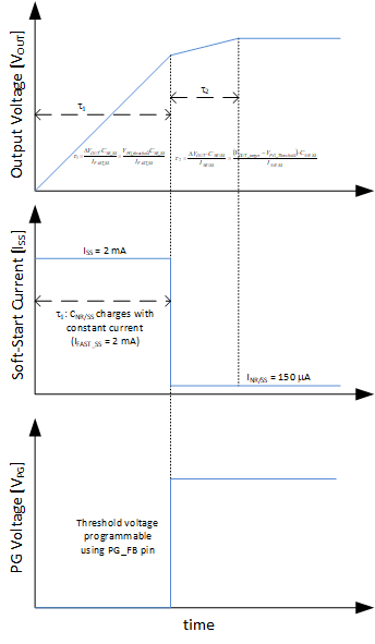
Figure 8-13 shows the relationship, timing, and output voltage value during the start-up phase.
 Figure 8-13 Relationship Between Threshold
Voltage, Output Voltage, IFAST_SS, and INR/SS During
Start-Up