JAJSP60 December   2022 TPS7B4255

PRODUCTION DATA  

  1. 特長
  2. アプリケーション
  3. 概要
  4. Revision History
  5. Pin Configuration and Functions
  6. Specifications
    1. 6.1 Absolute Maximum Ratings
    2. 6.2 ESD Ratings
    3. 6.3 Recommended Operating Conditions
    4. 6.4 Thermal Information
    5. 6.5 Electrical Characteristics
    6.     Timing Characteristics
    7. 6.6 Typical Characteristics
  7. Detailed Description
    1. 7.1 Overview
    2. 7.2 Functional Block Diagram
    3. 7.3 Feature Description
      1. 7.3.1 Regulated Output (VOUT)
      2. 7.3.2 Undervoltage Lockout
      3. 7.3.3 Thermal Protection
      4. 7.3.4 Current Limit
      5. 7.3.5 VOUT Short to Battery
      6. 7.3.6 Tracking Regulator With an Enable Circuit
    4. 7.4 Device Functional Modes
      1. 7.4.1 Operation With VIN < 3 V
      2. 7.4.2 Operation With ADJ/EN Control
  8. Application and Implementation
    1. 8.1 Application Information
      1. 8.1.1 Dropout Voltage
      2. 8.1.2 Reverse Current
      3. 8.1.3 Signal-Buffering LDO
    2. 8.2 Typical Application
      1. 8.2.1 Design Requirements
      2. 8.2.2 Detailed Design Procedure
        1. 8.2.2.1 Input and Output Capacitor Selection
      3. 8.2.3 Application Curves
    3. 8.3 Power Supply Recommendations
    4. 8.4 Layout
      1. 8.4.1 Layout Guidelines
        1. 8.4.1.1 Package Mounting
        2. 8.4.1.2 Board Layout Recommendations to Improve PSRR and Noise Performance
        3. 8.4.1.3 Power Dissipation and Thermal Considerations
        4. 8.4.1.4 Thermal Performance Versus Copper Area
      2. 8.4.2 Layout Example
  9. Device and Documentation Support
    1. 9.1 Device Support
      1. 9.1.1 Device Nomenclature
      2. 9.1.2 Development Support
    2. 9.2 ドキュメントの更新通知を受け取る方法
    3. 9.3 サポート・リソース
    4. 9.4 Trademarks
    5. 9.5 静電気放電に関する注意事項
    6. 9.6 用語集
  10. 10Mechanical, Packaging, and Orderable Information

パッケージ・オプション

メカニカル・データ(パッケージ|ピン)
サーマルパッド・メカニカル・データ
発注情報

Current Limit

The device has an internal current limit circuit to protect the device during overcurrent or shorting conditions. The current limit circuit, as shown in #GUID-E71E7299-4F59-45B8-AAE3-4B7E9B2092E2, is a brick-wall scheme. When the device is in current limit, the device sources ICL and the output voltage is not regulated. In this scenario, the output voltage depends on the load impedance.

During a current limit event, the potential for high power dissipation exists because of the elevated current level and the increased input-to-output differential voltage (VIN – VOUT). If the device heats enough, the device can enter thermal shutdown. If the current-limit condition is not removed when the device turns back on after cooling, the device can enter thermal shutdown again and continue this cycle until the current limit condition is removed. The device survives this fault, but repeatedly operating in this mode degrades long-term reliability.
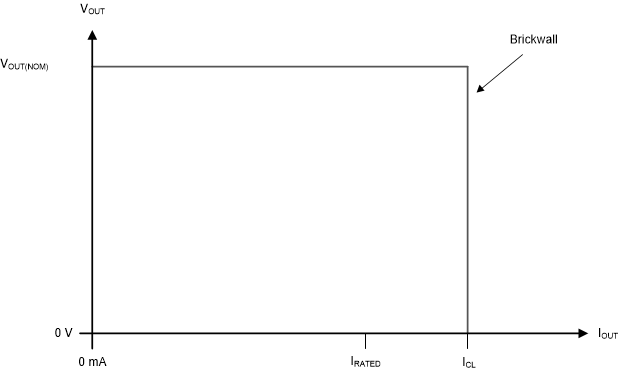
GUID-14337015-8638-4C98-A3E1-0F7AD1633EA8-low.gif Figure 7-2 Current Limit: Brick-Wall Scheme