SLVSAS4J June 2013 – April 2017 TPS7H1201-HT
PRODUCTION DATA.
- 1 Features
- 2 Applications
- 3 Description
- 4 Revision History
- 5 Pin Configuration and Functions
- 6 Specifications
- 7 Detailed Description
- 8 Application and Implementation
- 9 Power Supply Recommendations
- 10Layout
- 11Device and Documentation Support
- 12Mechanical, Packaging, and Orderable Information
パッケージ・オプション
メカニカル・データ(パッケージ|ピン)
- HKS|16
- KGD|0
サーマルパッド・メカニカル・データ
発注情報
7 Detailed Description
7.1 Overview
The TPS7H1201-HT is a 0.5-A, 1.5- to 7-V LDO linear regulator that uses PMOS pass element configuration.
It uses TI’s proprietary process to achieve low noise, high PSRR combined with high thermal performance in a 16-terminal ceramic flatpack package (HKS) or KGD (bare die) package.
A number of features are incorporated in the design to provide high reliability and system flexibility. Overload protection is incorporated in the design to make it viable for harsh environments.
A resistor connected from the PCL terminal to ground sets the current limit activation point. When current limit activation point is reached, output voltage drops while output load current is maintained at current limit point.
The device also has a current sense monitoring feature. A resistor connected from the CS terminal to VIN indicates voltage proportional to the output load current. PCL provides a detailed description of this feature.
To provide system flexibility for demanding current needs, the LDO can be configured in parallel operation as indicated in Figure 24. Current Sharing provides detailed parallel operation information.
An enable feature is incorporated in the design allowing the user to enable or disable the LDO. Power Good, an open-drain connection, indicates the status of the output voltage. These provide the customers' system flexibility in monitoring and controlling the LDO operation. When using the Enable function, VIN voltage must be > 3.5 V. For VIN from 1.5 to 7 V, TPS7H1201-HT can be disabled using the SS terminal as described in Enable/Disable.
7.2 Functional Block Diagram
 Figure 10. Block Diagram
7.3 Feature Description
7.3.1 Soft Start
Connecting a capacitor from the SS terminal to GND (CSS) slows down the output voltage ramp rate. The soft-start capacitor charges up to 1.2 V.

where
- tss = Soft-start time
- Iss = 2.5 µA
- VFB = VREF / 2 = 0.605 V
7.3.2 Power Good (PG)
Power Good terminal (9) is an open-drain connection and can be used to sequence multiple LDOs. Figure 11 shows typical connection for VIN > 3.5 V. The PG terminal will be pulled low until the output voltage reaches 90% of its maximum level. At that point, the PG pin will be pulled up. Since the PG pin is open drain, it can be pulled up to any voltage as long as it does not exceed the absolute max of 7.5 V listed in the table.
 Figure 11. Sequencing LDOs with Power Good
NOTE
For PSpice models, WEBENCH, and mini-POL reference design, see the Tools & Software tab.
- PSpice average model (stability – bode plot)
- PSpice transient model (switching waveforms)
- WEBENCH design tool (www.ti.com/product/TPS7H1201-HT/toolssoftware)
7.4 Device Functional Modes
7.4.1 Enable/Disable
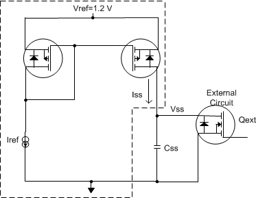
For VIN from 1.5 V to 7 V, TPS7H1201-HT can be disabled using the SS terminal. The minimum soft-start pulldown current is 10 μA, with soft start to ground voltage of 400 mV or lower. External voltage applied to the SS terminal must be limited to 1.2-V maximum. Removing the logic-low condition on soft start enables the device allowing the soft-start capacitor to get charged by the internal current source. Alternatively, for VIN > 3.5 V, the device can be disabled by pulling the enable terminal to logic low. In all other cases, the enable terminal should be connected to VIN.
 Figure 12. Enable/Disable
The circuit shown in Figure 12 highlights the SS terminal 1 along with block diagram of internal circuitry. Circuitry in dashed outline is internal to the IC composed of PMOSFET current mirror. The PMOS current mirror sources current from the positive supply and external circuitry composed of Qext is used to sink current from SS terminal 1. As highlighted in the table, typical ISS = 2.5 μA and max ISS = 3.5 μA for TPS7H1101-SP. If ISS current is exceeded, such as sinking higher current in excess of max ISS, this disables the LDO. See the table for the external sink current from SS terminal necessary to disable the IC. Exceeding maximum external sink current does not damage the device.