JAJSM19B May 2021 – December 2022 TPS7H4002-SP
PRODUCTION DATA
- 1 特長
- 2 アプリケーション
- 3 概要
- 4 Revision History
- 5 Pin Configuration and Functions
- 6 Specifications
-
7 Detailed Description
- 7.1 Overview
- 7.2 Functional Block Diagram
- 7.3
Feature Description
- 7.3.1 VIN and Power VIN Pins (VIN and PVIN)
- 7.3.2 Voltage Reference
- 7.3.3 Adjusting the Output Voltage
- 7.3.4 Safe Start-Up Into Prebiased Outputs
- 7.3.5 Error Amplifier
- 7.3.6 Slope Compensation
- 7.3.7 Enable and Adjust UVLO
- 7.3.8 Adjustable Switching Frequency and Synchronization (SYNC)
- 7.3.9 Slow Start (SS/TR)
- 7.3.10 Power Good (PWRGD)
- 7.3.11 Sequencing (SS/TR)
- 7.3.12 Output Overvoltage Protection (OVP)
- 7.3.13 Overcurrent Protection
- 7.3.14 Thermal Shutdown
- 7.3.15 Turn-On Behavior
- 7.3.16 Small Signal Model for Frequency Compensation
- 7.4 Device Functional Modes
-
8 Application and Implementation
- 8.1 Application Information
- 8.2
Typical Application
- 8.2.1 Design Requirements
- 8.2.2
Detailed Design Procedure
- 8.2.2.1 Operating Frequency
- 8.2.2.2 Output Inductor Selection
- 8.2.2.3 Output Capacitor Selection
- 8.2.2.4 Output Schottky Diode
- 8.2.2.5 Slow Start Capacitor Selection
- 8.2.2.6 Undervoltage Lockout (UVLO) Set Point
- 8.2.2.7 Output Voltage Feedback Resistor Selection
- 8.2.2.8 Compensation Component Selection
- 8.2.3 Parallel Operation
- 8.2.4 Application Curve
- 9 Power Supply Recommendations
- 10Layout
- 11Device and Documentation Support
- 12Mechanical, Packaging, and Orderable Information
パッケージ・オプション
メカニカル・データ(パッケージ|ピン)
- HKH|20
- KGD|0
サーマルパッド・メカニカル・データ
発注情報
7.3.8 Adjustable Switching Frequency and Synchronization (SYNC)
The switching frequency of the device supports three modes of operations. The modes of operation are set by the conditions on the RT and SYNC pins. At a high level, these modes can be described as primary-secondary, internal oscillator, and external synchronization modes.
In primary-secondary mode, the RT pin of the primary device should be left floating; the internal oscillator is set to 500 kHz, and the SYNC pin is set as an output clock. The SYNC output is in phase with respect to the internal oscillator of the primary device. SYNC out signal level is the same as VIN level with 50% duty cycle. SYNC signal feeding the secondary module, which is in phase with the primary clock, gets internally inverted (180° out of phase with the primary clock) internally in the secondary module. When trying to parallel with another converter, the RT pin of the second (secondary) converter must have its RT pin populated such that the converter frequency of the secondary converter must be within ±5% of the primary converter. This is required because the RT pin also sets the proper operation of slope compensation.
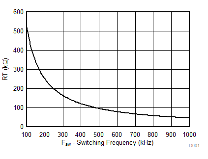
In internal oscillator mode, a resistor is connected between the RT pin and GND. The SYNC pin requires a 10-kΩ resistor to GND for this mode to be effective. The switching frequency of the device is adjustable from 100 kHz to 1 MHz by placing a maximum of 510 kΩ and a minimum of 47 kΩ respectively. To determine the RT resistance for a given switching frequency, use Equation 4 or the curve in Figure 7-4. To reduce the solution size, the designer should set switching frequency as high as possible, but consider the tradeoffs of supply efficiency and minimum controllable on-time.

where
- RT in kΩ
- FSW in kHz
 Figure 7-4 RT vs Switching Frequency
In external synchronization mode, a resistor is connected between the RT pin and GND. The SYNC pin requires a toggling signal for this mode to be effective. The switching frequency of the device goes 1:1 with that of SYNC pin. External system clock-user supplied sync clock signal determines the switching frequency. If no external clock signal is detected for 20 µs, then TPS7H4002-SP transitions to its internal clock, which is typically 500 kHz. An external synchronization using an inverter to obtain phase inversion is necessary. RT values of the primary and secondary converter must be within ±5% of the external synchronization frequency. This is necessary for proper slope compensation. A resistance in the RT pin is required for proper operation of the slope compensation circuit. To determine the RT resistance for a given switching frequency, use Equation 4 or the curve in Figure 7-4.
These modes are described in Table 7-1.
| RT PIN | SYNC PIN | SWITCHING FREQUENCY | DESCRIPTION AND NOTES |
|---|---|---|---|
| Float | Generates an output signal | 500 kHz | SYNC pin behaves as an output. SYNC output signal is in phase with the internal 500-kHz switching frequency. |
| 47-kΩ to 510-kΩ resistor to AGND | 10-kΩ resistor to GND | 100 kHz to 1 MHz | Internally generated switching frequency is based upon the resistor value present at the RT pin. |
| User-supplied sync clock or TPS7H4002-SP primary device sync output | Internally synchronized to external clock. External clock is inverted internally. | Set value of RT that corresponds to the externally supplied sync frequency. |