SLVSCE3A June 2014 – June 2014 TPS82740A , TPS82740B
PRODUCTION DATA.
- 1 Features
- 2 Applications
- 3 Description
- 4 Revision History
- 5 Device Comparison Table
- 6 Pin Configuration and Functions
- 7 Specifications
- 8 Parameter Measurement Information
- 9 Detailed Description
- 10Application and Implementation
- 11Power Supply Recommendations
- 12Layout
- 13Device and Documentation Support
- 14Mechanical, Packaging, and Orderable Information
パッケージ・オプション
デバイスごとのパッケージ図は、PDF版データシートをご参照ください。
メカニカル・データ(パッケージ|ピン)
- SIP|9
サーマルパッド・メカニカル・データ
発注情報
12.2 Layout Example
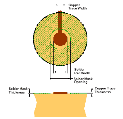
 Figure 46. Recommended Land Pattern Image and Dimensions
 | SOLDER PAD DEFINITIONS(1)(2)(3)(4) | COPPER PAD | SOLDER MASK (5)
OPENING |
COPPER THICKNESS | STENCIL (6)
OPENING |
STENCIL THICKNESS |
|---|---|---|---|---|---|
| Non-solder-mask defined (NSMD) | 0.30mm | 0.360mm | 1oz max (0.032mm) | 0.34mm diameter | 0.1mm thick |
(1) Circuit traces from non-solder-mask defined PWB lands should be 75μm to 100μm wide in the exposed area inside the solder mask opening. Wider trace widths reduce device stand off and affect reliability.
(2) Best reliability results are achieved when the PWB laminate glass transition temperature is above the operating the range of the intended application.
(3) Recommend solder paste is Type 3 or Type 4.
(4) For a PWB using a Ni/Au surface finish, the gold thickness should be less than 0.5mm to avoid a reduction in thermal fatigue performance.
(5) Solder mask thickness should be less than 20 μm on top of the copper circuit pattern.
(6) For best solder stencil performance use laser cut stencils with electro polishing. Chemically etched stencils give inferior solder paste volume control.
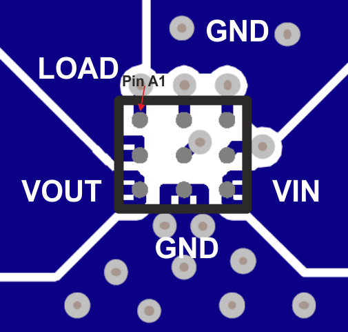
 Figure 47. PCB Layout Suggestion