JAJSF89C March 2013 – December 2019 TPS84A20
PRODUCTION DATA.
- 1 特長
- 2 アプリケーション
- 3 概要
- 4 改訂履歴
- 5 概要(続き)
- 6 Ordering Information
- 7 Specifications
- 8 Device Information
- 9 Typical Characteristics (PVIN = VIN = 12 V)
- 10Typical Characteristics (PVIN = VIN = 5 V)
- 11Typical Characteristics (PVIN = 3.3 V, VIN = 5 V)
-
12Application Information
- 12.1 Adjusting the Output Voltage
- 12.2 Capacitor Recommendations for the TPS84A20 Power Supply
- 12.3 Transient Response
- 12.4 Transient Waveforms
- 12.5 Application Schematics
- 12.6 VIN and PVIN Input Voltage
- 12.7 3.3 V PVIN Operation
- 12.8 Power Good (PWRGD)
- 12.9 Light Load Efficiency (LLE)
- 12.10 SYNC_OUT
- 12.11 Parallel Operation
- 12.12 Power-Up Characteristics
- 12.13 Pre-Biased Start-Up
- 12.14 Remote Sense
- 12.15 Thermal Shutdown
- 12.16 Output On/Off Inhibit (INH)
- 12.17 Slow Start (SS/TR)
- 12.18 Overcurrent Protection
- 12.19 Synchronization (CLK)
- 12.20 Sequencing (SS/TR)
- 12.21 Programmable Undervoltage Lockout (UVLO)
- 12.22 Layout Considerations
- 12.23 EMI
- 13デバイスおよびドキュメントのサポート
- 14メカニカル、パッケージ、および注文情報
パッケージ・オプション
デバイスごとのパッケージ図は、PDF版データシートをご参照ください。
メカニカル・データ(パッケージ|ピン)
- RVQ|42
サーマルパッド・メカニカル・データ
発注情報
12.12 Power-Up Characteristics
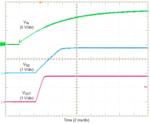
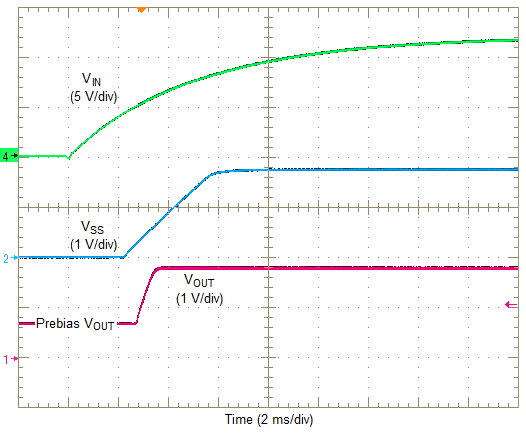
When configured as shown in the front page schematic, the TPS84A20 produces a regulated output voltage following the application of a valid input voltage. During the power-up, internal soft-start circuitry slows the rate that the output voltage rises, thereby limiting the amount of in-rush current that can be drawn from the input source. Figure 27 shows the start-up waveforms for a TPS84A20, operating from a 5-V input (PVIN = VIN) and with the output voltage adjusted to 1.8 V. Figure 28 shows the start-up waveforms for a TPS84A20 starting up into a pre-biased output voltage. The waveforms were measured with a 5-A constant current load.
 Figure 27. Start-Up Waveforms
  Figure 28. Start-up into Pre-bias