JAJSJ57B May   2020  – January 2022 TPS92200

PRODUCTION DATA  

  1. 特長
  2. アプリケーション
  3. 概要
  4. Revision History
  5. Pin Configuration and Functions
  6. Specifications
    1. 6.1 Absolute Maximum Ratings
    2. 6.2 ESD Ratings
    3. 6.3 Recommended Operating Conditions
    4. 6.4 Thermal Information
    5. 6.5 Electrical Characteristics
    6. 6.6 Timing Requirements
    7.     Switching Characteristics
    8. 6.7 Typical Characteristics
  7. Detailed Description
    1. 7.1 Overview
    2. 7.2 Functional Block Diagram
    3. 7.3 Feature Description
      1. 7.3.1 Peak-Current-Mode PWM Control
      2. 7.3.2 Setting LED Current
      3. 7.3.3 Internal Soft Start
      4. 7.3.4 Input Undervoltage Lockout
      5. 7.3.5 Bootstrap Regulator
      6. 7.3.6 Maximum Duty Cycle
      7. 7.3.7 Overcurrent Protection
        1. 7.3.7.1 High-Side MOSFET Overcurrent Protection
        2. 7.3.7.2 Low-Side MOSFET Sourcing Overcurrent Protection
        3. 7.3.7.3 Low-Side MOSFET Sinking Overcurrent Protection
      8. 7.3.8 Fault Protection
        1. 7.3.8.1 LED Open-Load Protection
        2. 7.3.8.2 LED+ and LED– Short Circuit Protection
        3. 7.3.8.3 LED+ Short Circuit to GND Protection
        4. 7.3.8.4 Sense-Resistor Open-Load Protection
        5. 7.3.8.5 Sense Resistor Short Circuit-to-GND Protection
        6. 7.3.8.6 Overvoltage Protection
        7. 7.3.8.7 Thermal Shutdown
    4. 7.4 Device Functional Modes
      1. 7.4.1 Enable and Disable the Device
      2. 7.4.2 TPS92200D1 PWM Dimming
      3. 7.4.3 TPS92200D1 Analog Dimming
      4. 7.4.4 TPS92200D2 Analog Dimming
  8. Application and Implementation
    1. 8.1 Application Information
    2. 8.2 Typical Application
      1. 8.2.1 TPS92200D1 12-V Input, 1.5-A, 2-Piece IR LED Driver With Analog Dimming
        1. 8.2.1.1 Design Requirements
        2. 8.2.1.2 Detailed Design Procedure
          1. 8.2.1.2.1 Inductor Selection
          2. 8.2.1.2.2 Input Capacitor Selection
          3. 8.2.1.2.3 Output Capacitor Selection
            1. 8.2.1.2.3.1 Sense Resistor Selection
              1. 8.2.1.2.3.1.1 Other External Components Selection
        3. 8.2.1.3 Application Curves
      2. 8.2.2 TPS92200D1 24-V Input, 1-A, 6-Piece WLED Driver With PWM Dimming
        1. 8.2.2.1 Design Requirements
        2. 8.2.2.2 Detailed Design Procedure
          1. 8.2.2.2.1 Inductor Selection
          2. 8.2.2.2.2 Input Capacitor Selection
          3. 8.2.2.2.3 Output Capacitor Selection
            1. 8.2.2.2.3.1 Sense Resistor Selection
              1. 8.2.2.2.3.1.1 Other External Components Selection
        3. 8.2.2.3 Application Curves
      3. 8.2.3 5-V Input, 1-A, 1-Piece IR LED Driver With TPS92200D2
        1. 8.2.3.1 Design Requirements
        2. 8.2.3.2 Detailed Design Procedure
          1. 8.2.3.2.1 Inductor Selection
          2. 8.2.3.2.2 Input Capacitor Selection
          3. 8.2.3.2.3 Output Capacitor Selection
            1. 8.2.3.2.3.1 Sense Resistor Selection
              1. 8.2.3.2.3.1.1 Other External Components Selection
        3. 8.2.3.3 Application Curves
  9. Power Supply Recommendations
  10. 10Layout
    1. 10.1 Layout Guidelines
    2. 10.2 Layout Example
  11. 11Device and Documentation Support
    1. 11.1 Receiving Notification of Documentation Updates
    2. 11.2 サポート・リソース
    3. 11.3 Trademarks
    4. 11.4 Electrostatic Discharge Caution
    5. 11.5 Glossary
  12. 12Mechanical, Packaging, and Orderable Information

パッケージ・オプション

メカニカル・データ(パッケージ|ピン)
サーマルパッド・メカニカル・データ
発注情報

Pin Configuration and Functions

Figure 5-1 DDC Package6-Pin SOT-23-THINTop View
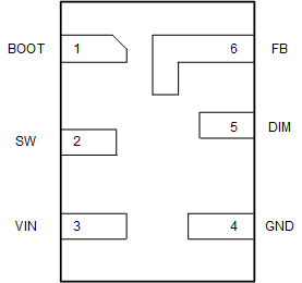
GUID-20210823-SS0I-S98R-WWB8-GZKSRXRWFWC7-low.gif Figure 5-2 RXL Package6-Pin VQFN-HRTop View
Table 5-1 Pin Functions
PIN TYPE(1) DESCRIPTION
NAME DDC NO. RXL NO.
BOOT 6 1 O A bootstrap capacitor is required between BOOT and SW.
FB 1 6 I LED current detection feedback
GND 3 4 G Power ground
DIM 2 5 I Dimming input. In PWM dimming mode, LED current is turned ON and OFF according to PWM duty cycle periodically (TPS92200D1). In analog dimming mode, the internal reference is proportional to the analog voltage on DIM pin (TPS92200D1) or the PWM duty input (TPS92200D2).
SW 5 2 O Switching node to external inductor
VIN 4 3 P Input supply voltage
I = Input, O = Output, P = Supply, G = Ground