JAJSFQ6E March 2014 – July 2018 TPS92601-Q1 , TPS92602-Q1
UNLESS OTHERWISE NOTED, this document contains PRODUCTION DATA.
- 1 特長
- 2 アプリケーション
- 3 概要
- 4 改訂履歴
- 5 Pin Configuration and Functions
- 6 Specifications
-
7 Detailed Description
- 7.1 Overview
- 7.2 Functional Block Diagram
- 7.3
Feature Description
- 7.3.1 Fixed-Frequency PWM Control
- 7.3.2 Slope-Compensation Output Current
- 7.3.3 Boost-Current Limit
- 7.3.4 Oscillator and PLL
- 7.3.5 Control Loop Compensation
- 7.3.6 LED Open-Circuit Detection
- 7.3.7 Output Short-Circuit and Overcurrent Detection
- 7.3.8 Measuring LED Current During a Non-Failure Condition
- 7.3.9 LED Dimming Options
- 7.4 Device Functional Modes
-
8 Application and Implementation
- 8.1 Application Information
- 8.2
Typical Applications
- 8.2.1
Boost Regulator With Separate or Paralleled Channels
- 8.2.1.1 Design Requirements
- 8.2.1.2
Detailed Design Procedure
- 8.2.1.2.1 Switching Frequency
- 8.2.1.2.2 Maximum Output-Current Set Point
- 8.2.1.2.3 Output Overvoltage-Protection Set Point
- 8.2.1.2.4 Duty Cycle Estimation
- 8.2.1.2.5 Inductor Selection
- 8.2.1.2.6 Rectifier Diode Selection
- 8.2.1.2.7 Output Capacitor Selection
- 8.2.1.2.8 Input Capacitor Selection
- 8.2.1.2.9 Current Sense and Current Limit
- 8.2.1.2.10 Switching MOSFET Selection
- 8.2.1.2.11 Loop Compensation
- 8.2.1.3 Application Curves
- 8.2.2
Boost-to-Battery Regulator
- 8.2.2.1 Design Requirements
- 8.2.2.2
Detailed Design Procedure
- 8.2.2.2.1 Switching Frequency
- 8.2.2.2.2 Maximum Output-Current Set Point
- 8.2.2.2.3 Output Overvoltage-Protection Set Point
- 8.2.2.2.4 Duty Cycle Estimation
- 8.2.2.2.5 Inductor Selection
- 8.2.2.2.6 Rectifier Diode Selection
- 8.2.2.2.7 Output Capacitor Selection
- 8.2.2.2.8 Input Capacitor Selection
- 8.2.2.2.9 Current Sense and Current Limit
- 8.2.2.2.10 Switching MOSFET Selection
- 8.2.2.2.11 Loop Compensation
- 8.2.2.3 TPS92602y-Q1 Application Curves
- 8.2.1
Boost Regulator With Separate or Paralleled Channels
- 9 Power Supply Recommendations
- 10Layout
- 11デバイスおよびドキュメントのサポート
- 12メカニカル、パッケージ、および注文情報
パッケージ・オプション
メカニカル・データ(パッケージ|ピン)
- PWP|20
サーマルパッド・メカニカル・データ
- PWP|20
発注情報
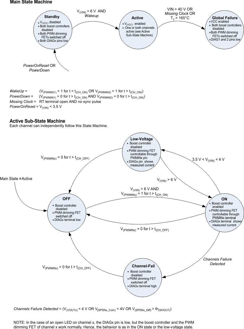
7.4.3 Device State Diagram
Figure 13 shows the state diagram of the device, with a short description of the device behavior in each state.
 Figure 13. Device State Diagram