JAJSFQ6E March 2014 – July 2018 TPS92601-Q1 , TPS92602-Q1
UNLESS OTHERWISE NOTED, this document contains PRODUCTION DATA.
- 1 特長
- 2 アプリケーション
- 3 概要
- 4 改訂履歴
- 5 Pin Configuration and Functions
- 6 Specifications
-
7 Detailed Description
- 7.1 Overview
- 7.2 Functional Block Diagram
- 7.3
Feature Description
- 7.3.1 Fixed-Frequency PWM Control
- 7.3.2 Slope-Compensation Output Current
- 7.3.3 Boost-Current Limit
- 7.3.4 Oscillator and PLL
- 7.3.5 Control Loop Compensation
- 7.3.6 LED Open-Circuit Detection
- 7.3.7 Output Short-Circuit and Overcurrent Detection
- 7.3.8 Measuring LED Current During a Non-Failure Condition
- 7.3.9 LED Dimming Options
- 7.4 Device Functional Modes
-
8 Application and Implementation
- 8.1 Application Information
- 8.2
Typical Applications
- 8.2.1
Boost Regulator With Separate or Paralleled Channels
- 8.2.1.1 Design Requirements
- 8.2.1.2
Detailed Design Procedure
- 8.2.1.2.1 Switching Frequency
- 8.2.1.2.2 Maximum Output-Current Set Point
- 8.2.1.2.3 Output Overvoltage-Protection Set Point
- 8.2.1.2.4 Duty Cycle Estimation
- 8.2.1.2.5 Inductor Selection
- 8.2.1.2.6 Rectifier Diode Selection
- 8.2.1.2.7 Output Capacitor Selection
- 8.2.1.2.8 Input Capacitor Selection
- 8.2.1.2.9 Current Sense and Current Limit
- 8.2.1.2.10 Switching MOSFET Selection
- 8.2.1.2.11 Loop Compensation
- 8.2.1.3 Application Curves
- 8.2.2
Boost-to-Battery Regulator
- 8.2.2.1 Design Requirements
- 8.2.2.2
Detailed Design Procedure
- 8.2.2.2.1 Switching Frequency
- 8.2.2.2.2 Maximum Output-Current Set Point
- 8.2.2.2.3 Output Overvoltage-Protection Set Point
- 8.2.2.2.4 Duty Cycle Estimation
- 8.2.2.2.5 Inductor Selection
- 8.2.2.2.6 Rectifier Diode Selection
- 8.2.2.2.7 Output Capacitor Selection
- 8.2.2.2.8 Input Capacitor Selection
- 8.2.2.2.9 Current Sense and Current Limit
- 8.2.2.2.10 Switching MOSFET Selection
- 8.2.2.2.11 Loop Compensation
- 8.2.2.3 TPS92602y-Q1 Application Curves
- 8.2.1
Boost Regulator With Separate or Paralleled Channels
- 9 Power Supply Recommendations
- 10Layout
- 11デバイスおよびドキュメントのサポート
- 12メカニカル、パッケージ、および注文情報
パッケージ・オプション
メカニカル・データ(パッケージ|ピン)
- PWP|28
サーマルパッド・メカニカル・データ
- PWP|28
発注情報
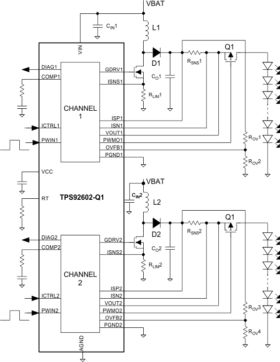
8.2.1 Boost Regulator With Separate or Paralleled Channels
A boost application is appropriate for a situation where V(VIN) is from 9 V to 16 V and LED forward voltage is always higher than battery the battery voltage. One can use the boost-regulator topology with each channel driving a separate LED string. For higher-current applications, connect both channels in parallel to drive a single LED string. The per-channel design parameters and calculations are the same in either case.
 Figure 14. Boost Regulator (VIN < VO) Simplified Schematic, Separate Channels
  Figure 15. Boost Regulator (VIN < VO) Simplified Schematic, Paralleled Channels
  Figure 16. Boost Regulator (VIN < VO) Detailed Schematic