JAJSHS0C March 2019 – March 2021 TPS92682-Q1
PRODUCTION DATA
- 1 特長
- 2 アプリケーション
- 3 概要
- 4 Revision History
- 5 Pin Configuration and Functions
- 6 Specifications
-
7 Detailed Description
- 7.1 Overview
- 7.2 Functional Block Diagram
- 7.3
Feature Description
- 7.3.1 Device Enable
- 7.3.2 Internal Regulator and Undervoltage Lockout (UVLO)
- 7.3.3 Oscillator
- 7.3.4 Spread Spectrum Function
- 7.3.5 Gate Driver
- 7.3.6 Rail-to-Rail Current Sense Amplifier
- 7.3.7 Transconductance Error Amplifier
- 7.3.8 Switch Current Sense
- 7.3.9 Slope Compensation
- 7.3.10 ILED Setting in CC Mode
- 7.3.11 Output Voltage Setting in CV Mode
- 7.3.12 PWM Dimming
- 7.3.13 P-Channel FET Gate Driver Output
- 7.3.14 Soft Start
- 7.3.15 Two-Phase Operation
- 7.3.16 Faults and Diagnostics
- 7.4 Device Functional Modes
- 7.5 Programming
- 7.6
TPS92682 Registers
- 7.6.1 EN Register
- 7.6.2 CFG1 Register
- 7.6.3 CFG2 Register
- 7.6.4 SWDIV Register
- 7.6.5 ISLOPE Register
- 7.6.6 FM Register
- 7.6.7 SOFTSTART Register
- 7.6.8 CH1IADJ Register
- 7.6.9 CH2IADJ Register
- 7.6.10 PWMDIV Register
- 7.6.11 CH1PWML Register
- 7.6.12 CH1PWMH Register
- 7.6.13 CH2PWML Register
- 7.6.14 CH2PWMH Register
- 7.6.15 ILIM Register
- 7.6.16 IFT Register
- 7.6.17 MFT Register
- 7.6.18 FLT1 Register (read only)
- 7.6.19 FLT2 Register (read only)
- 7.6.20 FEN1 Register
- 7.6.21 FEN2 Register
- 7.6.22 FLATEN Register
- 7.6.23 OV Register
- 7.6.24 LHCFG Register
- 7.6.25 LHCH1IADJ Register
- 7.6.26 LHCH2IADJ Register
- 7.6.27 LHCH1PWML Register
- 7.6.28 LHCH1PWMH Register
- 7.6.29 LHCH2PWML Register
- 7.6.30 LHCH2PWMH Register
- 7.6.31 LHILIM Register
- 7.6.32 LHIFT Register
- 7.6.33 LHMFT Register
- 7.6.34 LHFEN1 Register
- 7.6.35 LHFEN2 Register
- 7.6.36 LHFLATEN Register
- 7.6.37 LHOV Register
- 7.6.38 CAL Register
- 7.6.39 RESET Register
-
8 Application and Implementation
- 8.1 Application Information General Design Considerations
- 8.2 Application Information CC Mode
- 8.3 Typical Application CV Mode
- 8.4
Typical Application CC Mode
- 8.4.1 CC Boost Design Requirements
- 8.4.2
CC Boost Detailed Design Procedure
- 8.4.2.1 Calculating Duty Cycle
- 8.4.2.2 Setting Switching Frequency
- 8.4.2.3 Setting Dither Modulation Frequency
- 8.4.2.4 Inductor Selection
- 8.4.2.5 Output Capacitor Selection
- 8.4.2.6 Input Capacitor Selection
- 8.4.2.7 Main N-Channel MOSFET Selection
- 8.4.2.8 Rectifier Diode Selection
- 8.4.2.9 Setting ILED and Selecting RCS
- 8.4.2.10 Setting Switch Current Limit
- 8.4.2.11 Slope Compensation
- 8.4.2.12 Compensator Parameters
- 8.4.2.13 Overvoltage Protection
- 8.4.2.14 Series P-Channel MOSFET Selection
- 8.4.3 CC Buck-Boost Design Requirements
- 8.4.4
CC Buck-Boost Detailed Design Procedure
- 8.4.4.1 Calculating Duty Cycle
- 8.4.4.2 Setting Switching Frequency
- 8.4.4.3 Setting Dither Modulation Frequency
- 8.4.4.4 Inductor Selection
- 8.4.4.5 Output Capacitor Selection
- 8.4.4.6 Input Capacitor Selection
- 8.4.4.7 Main N-Channel MOSFET Selection
- 8.4.4.8 Rectifier Diode Selection
- 8.4.4.9 Setting ILED and Selecting RCS
- 8.4.4.10 Setting Switch Current Limit
- 8.4.4.11 Slope Compensation
- 8.4.4.12 Compensator Parameters
- 8.4.4.13 Overvoltage Protection
- 8.4.5 PWM Dimming Consideration
- 8.4.6 Application Curves
- 8.5
Typical Application CV Mode
- 8.5.1 CV Design Requirements
- 8.5.2
Detailed Design Procedure
- 8.5.2.1 Calculating Duty Cycle
- 8.5.2.2 Setting Switching Frequency
- 8.5.2.3 Setting Dither Modulation Frequency
- 8.5.2.4 Inductor Selection
- 8.5.2.5 Output Capacitor Selection
- 8.5.2.6 Input Capacitor Selection
- 8.5.2.7 Main N-Channel MOSFET Selection
- 8.5.2.8 Rectifier Diode Selection
- 8.5.2.9 Programming VOUT
- 8.5.2.10 Setting Switch Current Limit
- 8.5.2.11 Slope Compensation
- 8.5.2.12 Compensator Parameters
- 8.5.2.13 Overvoltage Protection
- 8.5.3 Application Curves
- 9 Power Supply Recommendations
- 10Layout
- 11Device and Documentation Support
- 12Mechanical, Packaging, and Orderable Information
パッケージ・オプション
メカニカル・データ(パッケージ|ピン)
サーマルパッド・メカニカル・データ
発注情報
7.3.7 Transconductance Error Amplifier
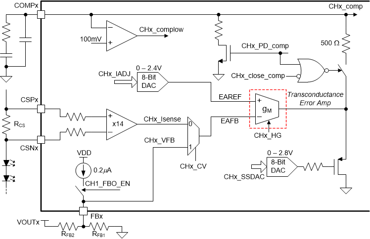
As shown in Figure 7-8, the internal transconductance error amplifier generates an error signal proportional to the difference between the internal programmable 8-bit CHxIADJ-DAC (CH1IADJ Register) and the feedback signal. The feedback signal is the sensed current CHxIsense in CC mode, or the sense output voltage, CHxVFB, in CV mode. The gain gM of the error amplifier is programmable through the CHx_HG bit in the CFG1 Register. The gain values for CHx_HG = 0 or 1 are provided in the Electrical Characteristics. Based on the value of CHx_CV bit in Table 7-4, either CHxIsense or CHxVFB is connected to the input of the error amplifier. Therefore, the TPS92682-Q1 device either operates in CV or CC mode.
The output of the error amplifier is connected to an external compensation network to achieve closed-loop LED current (CC), or output voltage (CV) regulation. In most LED driver applications, a simple integral compensation circuit consisting of a capacitor connected from COMPx output to GND provides a stable response over a wide range of operating conditions. TI recommends a capacitor value between 10 nF and 100 nF as a good starting point. To achieve higher closed-loop bandwidth, a proportional-integral compensator, consisting of a series resistor and a capacitor network connected across the COMPx output and GND, is required. Application and Implementation includes a summarized detailed design procedure.
 Figure 7-8 Feedback Connection to the Error Amplifier