-
TPS92692, TPS92692-Q1 High Accuracy LED Controller With Spread Spectrum Frequency Modulation
- 1 Features
- 2 Applications
- 3 Description
- 4 Revision History
- 5 Pin Configuration and Functions
- 6 Specifications
-
7 Detailed Description
- 7.1 Overview
- 7.2 Functional Block Diagram
- 7.3
Feature Description
- 7.3.1 Internal Regulator and Undervoltage Lockout (UVLO)
- 7.3.2 Oscillator
- 7.3.3 Spread Spectrum Frequency Modulation
- 7.3.4 Gate Driver
- 7.3.5 Rail-to-Rail Current Sense Amplifier
- 7.3.6 Transconductance Error Amplifier
- 7.3.7 Switch Current Sense
- 7.3.8 Slope Compensation
- 7.3.9 Analog Adjust Input
- 7.3.10 DIM/PWM Input
- 7.3.11 Series P-Channel FET Dimming Gate Driver Output
- 7.3.12 Soft-Start
- 7.3.13 Current Monitor Output
- 7.3.14 Output Overvoltage Protection
- 7.3.15 Output Short-circuit Protection
- 7.3.16 Thermal Protection
- 7.3.17 Fault Indicator (FLT)
- 7.4 Device Functional Modes
-
8 Application and Implementation
- 8.1
Application Information
- 8.1.1 Duty Cycle Considerations
- 8.1.2 Inductor Selection
- 8.1.3 Output Capacitor Selection
- 8.1.4 Input Capacitor Selection
- 8.1.5 Main Power MOSFET Selection
- 8.1.6 Rectifier Diode Selection
- 8.1.7 LED Current Programming
- 8.1.8 Switch Current Sense Resistor
- 8.1.9 Slope Compensation
- 8.1.10 Feedback Compensation
- 8.1.11 Soft-Start
- 8.1.12 Overvoltage and Undervoltage Protection
- 8.1.13 Analog to PWM Dimming Considerations
- 8.1.14 Direct PWM Dimming Considerations
- 8.1.15 Series P-Channel MOSFET Selection
- 8.2
Typical Applications
- 8.2.1
Typical Boost LED Driver
- 8.2.1.1 Design Requirements
- 8.2.1.2
Detailed Design Procedure
- 8.2.1.2.1 Calculating Duty Cycle
- 8.2.1.2.2 Setting Switching Frequency
- 8.2.1.2.3 Setting Dither Modulation Frequency
- 8.2.1.2.4 Inductor Selection
- 8.2.1.2.5 Output Capacitor Selection
- 8.2.1.2.6 Input Capacitor Selection
- 8.2.1.2.7 Main N-Channel MOSFET Selection
- 8.2.1.2.8 Rectifying Diode Selection
- 8.2.1.2.9 Programming LED Current
- 8.2.1.2.10 Setting Switch Current Limit
- 8.2.1.2.11 Programming Slope Compensation
- 8.2.1.2.12 Deriving Compensator Parameters
- 8.2.1.2.13 Setting Start-up Duration
- 8.2.1.2.14 Setting Overvoltage Protection Threshold
- 8.2.1.2.15 Analog-to-PWM Dimming Considerations
- 8.2.1.3 Application Curves
- 8.2.2
Typical Buck-Boost LED Driver
- 8.2.2.1 Design Requirements
- 8.2.2.2
Detailed Design Procedure
- 8.2.2.2.1 Calculating Duty Cycle
- 8.2.2.2.2 Setting Switching Frequency
- 8.2.2.2.3 Setting Dither Modulation Frequency
- 8.2.2.2.4 Inductor Selection
- 8.2.2.2.5 Output Capacitor Selection
- 8.2.2.2.6 Input Capacitor Selection
- 8.2.2.2.7 Main N-Channel MOSFET Selection
- 8.2.2.2.8 Rectifier Diode Selection
- 8.2.2.2.9 Programming LED Current
- 8.2.2.2.10 Setting Switch Current Limit and Slope Compensation
- 8.2.2.2.11 Programming Slope Compensation
- 8.2.2.2.12 Deriving Compensator Parameters
- 8.2.2.2.13 Setting Startup Duration
- 8.2.2.2.14 Setting Overvoltage Protection Threshold
- 8.2.2.2.15 Direct PWM Dimming Consideration
- 8.2.2.3 Application Curves
- 8.2.1
Typical Boost LED Driver
- 8.1
Application Information
- 9 Power Supply Recommendations
- 10Layout
- 11Device and Documentation Support
- 12Mechanical, Packaging, and Orderable Information
- IMPORTANT NOTICE
パッケージ・オプション
メカニカル・データ(パッケージ|ピン)
- PWP|20
サーマルパッド・メカニカル・データ
- PWP|20
発注情報
TPS92692, TPS92692-Q1 High Accuracy LED Controller With Spread Spectrum Frequency Modulation
1 Features
- Wide Input Voltage: 4.5 V to 65 V
- Better than ± 4% LED Current Accuracy over –40°C to 150°C Junction Temperature Range
- Spread Spectrum Frequency Modulation for Improved EMI
- Comprehensive Fault Protection Circuitry with Current Monitor output and Open Drain Fault Flag Indicator
- Internal Analog Voltage to PWM Duty Cycle Generator for stand-alone Dimming Operation
- Compatible with Direct PWM Input with over 1000:1 Dimming Range
- Analog LED Current Adjust Input (IADJ) with over 15:1 Contrast Ratio
- Integrated P-Channel Driver to enable Series FET Dimming and LED Protection
- TPS92692-Q1: Automotive Q100 Grade 1 Qualified
2 Applications
- TPS92692-Q1: Automotive Exterior Lighting Applications
- Driver Monitoring Systems (DMS)
- LED General Lighting Applications
- Exit Signs and Emergency Lighting
3 Description
The TPS92692 and TPS92692-Q1 are high accuracy peak current mode based controllers designed to support step-up/down LED driver topologies. The device incorporates a rail-to-rail current amplifier to measure LED current and spread spectrum frequency modulation technique for improved EMI performance.
This high performance LED controller can independently modulate LED current using either analog or PWM dimming techniques. Linear analog dimming response with over 15:1 range is obtained by varying the voltage across the high impedance analog adjust (IADJ) input. PWM dimming of LED current is achieved by directly modulating the DIM/PWM input pin with the desired duty cycle or by enabling the internal PWM generator circuit. The PWM generator translates the DC voltage at DIM/PWM pin to corresponding duty cycle by comparing it to the internal triangle wave generator. The optional PDRV gate driver output can be used to drive an external P-Channel series MOSFET.
The TPS92692 and TPS92692-Q1 devices support continuous LED status check through the current monitor (IMON) output. The devices also include an open drain fault indicator output to indicate LED overcurrent, output overvoltage and output undervoltage conditions.
Device Information(1)
| PART NUMBER | PACKAGE | BODY SIZE (NOM) |
|---|---|---|
| TPS92692-Q1 | HTSSOP (20) | 5.10 mm × 6.60 mm |
| TPS92692 |
- For all available packages, see the orderable addendum at the end of the data sheet.
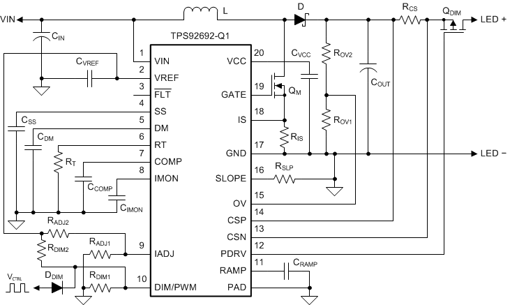
Typical Boost LED Driver
4 Revision History
| DATE | REVISION | NOTES |
|---|---|---|
| March 2017 | * | Initial release. |
5 Pin Configuration and Functions
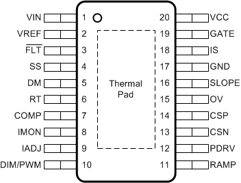
Pin Functions
| PIN | I/O | DESCRIPTION | |
|---|---|---|---|
| NAME | NO. | ||
| COMP | 7 | I/O | Transconductance error amplifier output. Connect compensation network to achieve desired closed-loop response. |
| CSN | 13 | I | Current sense amplifier negative input (–). Connect directly to the negative node of LED current sense resistor, RCS. |
| CSP | 14 | I | Current sense amplifier positive input (+). Connect directly to the positive node of LED current sense resistor, RCS. |
| DIM/PWM | 10 | I | External analog to PWM dimming command or direct PWM dimming input. The external analog dimming command between 1 V and 3 V is compared to the internal PWM generator triangle waveform to set LED current duty cycle between 0% and 100%. With PWM generator disabled, a direct PWM dimming command can be applied to control the LED current duty cycle and frequency. The analog or PWM command is used to generate an internal PWM signal that controls the GATE and PDRV outputs. Setting the internal PWM signal to logic level low, turns off switching, idles the oscillator, disconnects the COMP pin, and sets PDRV to VCSP. Connect to VREF when not used for PWM dimming. |
| DM | 5 | I/O | Triangle wave spread spectrum modulation frequency, fm, programming pin. Connect a capacitor to GND to set the spread spectrum modulating frequency. Connect directly to GND to disable spread spectrum modulation of switching frequency. |
| FLT | 3 | O | Open-drain fault indicator. Connect to VREF with a resistor to create active low fault signal output. Internal LED short circuit protection and auto-restart timer can enabled by directly connecting the pin to SS input. |
| GATE | 19 | O | N-channel MOSFET gate driver output. Connect to gate of external main switching N-channel MOSFET. |
| GND | 17 | — | Analog and Power ground connection pin. Connect to circuit ground to complete return path. |
| IADJ | 9 | I | LED current reference input. Connect this pin to VCC with a 100-kΩ series resistor to set the internal reference voltage to 2.42 V and the current sense threshold, V(CSP-CSN) to 170.7 mV. The pin can be modulated by an external voltage source from 140 mV to 2.25 V to implement analog dimming. |
| IMON | 8 | O | LED current report pin. The LED current sensed by CSP/CSN input is reported as VIMON = 14 × ILED × RCS. Bypass with a 1-nF ceramic capacitor connected to GND. |
| IS | 18 | I | Switch current sense input. Connect to the switch sense resistor, RIS to set the switch current limit threshold based on the internal 250 mV reference. |
| OV | 15 | I | Output voltage input. Connect a resistor divider from output voltage to GND to set output overvoltage and under-voltage protection thresholds. |
| PDRV | 12 | O | Series dimming P-channel FET gate driver output. Connect to gate of external P-channel MOSFET to implement series FET PWM dimming and fault disconnect. |
| RAMP | 11 | I/O | Programming input for internal PWM generator. Connect a capacitor to GND to set the triangle wave frequency for PWM generator circuit. Connect a 249-kΩ resistor to GND to disable the PWM generator and to set a fixed reference for direct external PWM dimming input. Do not allow this pin to float. |
| RT | 6 | I/O | Oscillator frequency programming pin. Connect a resistor to GND to set the switching frequency. The internal oscillator can be synchronized by coupling an external clock pulse through a series capacitor with a value of 100 nF. |
| SLOPE | 16 | I/O | Slope compensation input. Connect a resistor to GND to set the desired slope compensation ramp based on inductor value, input and output voltages. |
| SS | 4 | I/O | Soft-start programming pin. Connect a capacitor to GND to extend the start-up time. Switching can be disabled by shorting this pin to GND. |
| VCC | 20 | — | VCC (7.5 V) bias supply pin. Locally decouple to GND using a ceramic capacitor (with a value between 2.2-µF and 4.7-µF). Locate close to the controller. |
| VIN | 1 | — | Input supply for the internal regulators. Bypass with a low-pass filter using a series 10-Ω resistor and 10- nF capacitor connected to GND. Locate the capacitor close to the controller. |
| VREF | 2 | — | VREF (5 V) bias supply pin. Locally decouple to GND using a ceramic capacitor (with a value between 2.2-µF and 4.7-µF) located close to the controller. |
| Thermal Pad | — | The GND pin must be connected to the exposed thermal pad for proper operation. This PowerPAD must be connected to PCB ground plane using multiple vias for good thermal performance. | |
6 Specifications
6.1 Absolute Maximum Ratings
over operating free-air temperature range (unless otherwise noted)(1)(2)| MIN | MAX | UNIT | ||
|---|---|---|---|---|
| Input voltage | VIN, CSP, CSN | –0.3 | 65 | V |
| DIM/PWM | –0.3 | 14 | V | |
| IS, RT, FLT | –0.3 | 8.8 | V | |
| OV, SS, RAMP, DM, SLOPE, VREF, IADJ | –0.3 | 5.5 | V | |
| CSP to CSN(3) | –0.3 | 0.3 | V | |
| Output voltage(4) | VCC, GATE | –0.3 | 8.8 | V |
| PDRV | VCSP – 8.8 | VCSP | V | |
| COMP | –0.3 | 5.0 | V | |
| Source current | IMON | — | 100 | µA |
| GATE (pulsed < 20 ns) | — | 500 | mA | |
| PDRV (pulsed < 10 µs) | — | 50 | mA | |
| Sink current | GATE (pulsed < 20 ns) | — | 500 | mA |
| PDRV (pulsed < 10 µs) | — | 50 | mA | |
| Operating junction temperature, TJ | –40 | 150 | °C | |
| Storage temperature, Tstg | 165 | °C | ||
6.2 ESD Ratings
| VALUE | UNIT | ||||
|---|---|---|---|---|---|
| TPS92692-Q1 IN PWP (HTSSOP) PACKAGE | |||||
| V(ESD) | Electrostatic discharge | Human-body model (HBM), per AEC Q100-002, all pins(1) | ±2000 | V | |
| Charged-device model (CDM), per AEC Q100-011 | All pins except 1, 10, 11, and 20 | ±500 | |||
| Pins 1, 10, 11, and 20 | ±750 | ||||
| TPS92692 IN PWP (HTSSOP) PACKAGE | |||||
| V(ESD) | Electrostatic discharge | Human-body model (HBM), per ANSI/ESDA/JEDEC JS-001, all pins(2) | ±2000 | V | |
| Charged-device model (CDM), per JEDEC specification JESD22-C101, all pins(3) | ±500 | ||||
6.3 Recommended Operating Conditions
over operating free-air temperature range (unless otherwise noted)| MIN | NOM | MAX | UNIT | ||
|---|---|---|---|---|---|
| VIN | Supply input voltage | 6.5 | 14 | 65 | V |
| VIN, crank | Supply input, battery crank voltage | 4.5 | V | ||
| VCSP, VCSN | Current sense common mode | 6.5 | 60 | V | |
| ƒSW | Switching frequency | 80 | 800 | kHz | |
| ƒm | Spread spectrum modulation frequency | 0.1 | 12 | kHz | |
| fRAMP | Internal PWM ramp generator frequency | 100 | 2000 | Hz | |
| VIADJ | Current reference voltage | 0.14 | VIADJ(CLAMP) | V | |
| TA | Operating ambient temperature | –40 | 125 | °C | |
6.4 Thermal Information
| THERMAL METRIC(1) | TPS92692 | TPS92692-Q1 | UNIT | |
|---|---|---|---|---|
| PWP (HTSSOP) | PWP (HTSSOP) | |||
| 20 PINS | 20 PINS | |||
| RθJA | Junction-to-ambient thermal resistance | 40.8 | 40.8 | °C/W |
| RθJC(top) | Junction-to-case (top) thermal resistance | 26.1 | 26.1 | °C/W |
| RθJB | Junction-to-board thermal resistance | 22.2 | 22.2 | °C/W |
| ψJT | Junction-to-top characterization parameter | 0.8 | 0.8 | °C/W |
| ψJB | Junction-to-board characterization parameter | 22.0 | 22.0 | °C/W |
| RθJC(bot) | Junction-to-case (bottom) thermal resistance | 2.3 | 2.3 | °C/W |
6.5 Electrical Characteristics
–40°C ≤ TJ ≤ 150°C, VIN = 14 V, VIADJ = 2.1 V, VRAMP = 500 mV, VDIM/PWM = 3 V, VOV = 500 mV, CVCC = 1 µF, CVREF = 1 µF, CCOMP = 2.2 nF, RCS = 100 mΩ, RT = 20 kΩ, no load on GATE and PDRV (unless otherwise noted)(1)| PARAMETER | TEST CONDITIONS | MIN | TYP | MAX | UNIT | |
|---|---|---|---|---|---|---|
| INPUT VOLTAGE (VIN) | ||||||
| IIN(STBY) | Input stand-by current | VPWM = 0 V | 1.8 | 2.5 | mA | |
| IIN(SW) | Input switching current | VCC = 7.5 V, CGATE = 1 nF | 5.1 | 6.6 | mA | |
| BIAS SUPPLY (VCC) | ||||||
| VCC(REG) | Regulation voltage | No load | 7.0 | 7.5 | 8.0 | V |
| VCC(UVLO) | Supply undervoltage protection | VCC rising threshold, VIN = 8 V | 4.5 | 4.9 | V | |
| VCC falling threshold, VIN = 8 V | 3.7 | 4.1 | V | |||
| Hysteresis | 400 | mV | ||||
| ICC(LIMIT) | Supply current limit | VCC = 0 V | 30 | 36 | 46 | mA |
| VDO | LDO dropout voltage | ICC = 20 mA, VIN = 5 V | 300 | mV | ||
| REFERENCE VOLTAGE (VREF) | ||||||
| VREF | Reference voltage | No load | 4.77 | 4.96 | 5.15 | V |
| IREF(LIMIT) | Current limit | VREF = 0 V | 30 | 36 | 46 | mA |
| OSCILLATOR (RT) | ||||||
| ƒSW | Switching frequency | RT = 40 kΩ | 175 | 200 | 225 | kHz |
| RT = 20 kΩ | 341 | 390 | 439 | kHz | ||
| VRT | RT output voltage | 1 | V | |||
| VSYNC | SYNC rising threshold | VRT rising | 2.5 | 3.1 | V | |
| SYNC falling threshold | VRT falling | 1.8 | 2 | V | ||
| tSYNC(MIN) | Minimum SYNC clock pulse width | 100 | ns | |||
| SPREAD SPECTRUM FREQUENCY MODULATION (DM) | ||||||
| IDM | Triangle wave generator sink current | 10 | µA | |||
| Triangle wave generator source current | 10 | µA | ||||
| VDM(TR) | Triangle wave voltage peak (High) | 1.15 | V | |||
| Triangle wave voltage valley (Low) | 850 | mV | ||||
| VDM(EN) | Spread spectrum modulation enable threshold | 700 | mV | |||
| VDM(CLAMP) | Internal clamp voltage | VPWM = 0 V, RRAMP = 200 kΩ | 1.25 | V | ||
| GATE DRIVER (GATE) | ||||||
| RGH | Gate driver high side resistance | IGATE = –10 mA | 5.4 | 11.2 | Ω | |
| RGL | Gate driver low side resistance | IGATE = 10 mA | 4.3 | 10.5 | Ω | |
| CURRENT SENSE (IS) | ||||||
| VIS(LIMIT) | Current limit threshold | VDIM/PWM = 5 V, RRAMP = 249 kΩ | 230.6 | 250 | 270 | mV |
| VDIM/PWM = 0 V, RRAMP = 249 kΩ | 665 | 700 | 735 | mV | ||
| tIS(BLANK) | Leading edge blanking time | 88 | 118 | 158 | ns | |
| tIS(FAULT) | Current limit fault time | 35 | µs | |||
| tILMT(DLY) | IS to GATE propagation delay | VIS pulsed from 0 V to 1 V | 78 | ns | ||
| PWM COMPARATOR AND SLOPE COMPENSATION (SLOPE) | ||||||
| DMAX | Maximum duty cycle | 90 | % | |||
| VSLOPE | Adaptive slope compensation | VCSP = 24 V | 410 | mV | ||
| VSLOPE(MIN) | Minimum slope compensation output voltage | VCSP = 0 V | 72 | mV | ||
| VLV | IS to COMP level shift voltage | No slope compensation added | 1.42 | 1.60 | 1.82 | V |
| ILV | IS level shift bias current | No slope compensation added | 17 | µA | ||
| CURRENT SENSE AMPLIFIER (CSP, CSN) | ||||||
| V(CSP-CSN) | Current sense thresholds | VCSP = 14 V, VIADJ = 3 V | 163.4 | 170.7 | 177.6 | mV |
| VCSP = 14 V, VIADJ = 1.4 V | 95.83 | 100.5 | 103.85 | mV | ||
| CS(BW) | Current sense unity gain bandwidth | 500 | kHz | |||
| GCS | Current sense amplifier gain | G = VIADJ/V(CSP-CSN) | 14 | |||
| K(OCP) | Ratio of over-current detection threshold to analog adjust voltage | K (OCP) = V(OCP-THR)/VIADJ | 1.46 | 1.5 | 1.61 | |
| ICSP(BIAS) | CSP bias current | VCSN = 14.1 V, VCSP = 14 V | 107 | µA | ||
| ICSN(BIAS) | CSN bias current | VCSN = 14.1 V, VCSP = 14 V | 110 | µA | ||
| FAULT INDICATOR (FLT) | ||||||
| R(FLT) | Open-drain pull down resistance | 241 | Ω | |||
| t(FAULT_TMR) | Fault timer | 24 | 36 | 48 | ms | |
| CURRENT MONITOR (IMON) | ||||||
| IIMON(SRC) | IMON source current | V(CSP-CSN) = 150 mV, VIMON = 0 V |
144 | µA | ||
| VIMON(CLP) | IMON output voltage clamp | 3.2 | 3.7 | 4.2 | V | |
| VIMON(OS) | IMON buffer offset voltage | –7.2 | 0 | 8.5 | mV | |
| ANALOG ADJUST (IADJ) | ||||||
| VIADJ(CLP) | IADJ internal clamp voltage | IIADJ = 1 µA | 2.29 | 2.40 | 2.55 | V |
| IIADJ(BIAS) | IADJ input bias current | VIADJ < 2.2 V | 10.5 | nA | ||
| RIADJ(LMT) | IADJ current limiting series resistor | VIADJ > 2.6 V | 12 | kΩ | ||
| ERROR AMPLIFIER (COMP) | ||||||
| gM | Transconductance | 121 | µA/V | |||
| ICOMP(SRC) | COMP current source capacity | VIADJ = 1.4 V, V(CSP-CSN) = 0 V | 130 | µA | ||
| ICOMP(SINK) | COMP current sink capacity | VIADJ = 0 V, V(CSP-CSN) = 0.1 V | 130 | µA | ||
| EA(BW) | Error amplifier bandwidth | Gain = –3 dB | 5 | MHz | ||
| VCOMP(RST) | COMP pin reset voltage | 100 | mV | |||
| RCOMP(DCH) | COMP discharge FET resistance | 246 | Ω | |||
| SOFT-START (SS) | ||||||
| ISS | Soft-start source current | 7 | 10 | 12.8 | µA | |
| VSS(UVP_EN) | Soft-start voltage threshold to enable output under-voltage protection | 2.4 | V | |||
| VSS(RST) | Soft-start pin reset voltage | 50 | mV | |||
| RSS(DCH) | SS discharge FET resistance | 240 | Ω | |||
| OUTPUT VOLTAGE INPUT (OV) | ||||||
| VOVP(THR) | Overvoltage protection threshold | 1.195 | 1.228 | 1.262 | V | |
| VUVP(THR) | Undervoltage protection threshold | 81.7 | 100 | 115.1 | mV | |
| t(UVP-BLANK) | Undervoltage protection blanking period | 4 | µs | |||
| IOVP(HYS) | OVP hysteresis current | 12 | 20 | 27.5 | µA | |
| INTERNAL PWM RAMP GENERATOR (RAMP) | ||||||
| IRAMP | Ramp generator source current | 7.75 | 10 | 12.73 | µA | |
| Ramp generator sink current | 8.24 | 10 | 12.41 | µA | ||
| VRAMP | Ramp signal peak (high) | 3 | V | |||
| Ramp signal valley (low) | 1 | V | ||||
| PWM INPUT (DIM/PWM) | ||||||
| VPWM(HIGH) | Schmitt trigger logic level (high threshold) | VRAMP = 2.0 V | 2.0 | 2.2 | V | |
| VPWM(LOW) | Schmitt trigger logic level (low threshold) | VRAMP = 2.0 V | 1.8 | 2.0 | V | |
| RPWM(PD) | PWM pull-down resistance | 10 | MΩ | |||
| tDLY(RISE) | PWM rising to PDRV delay | CPDRV = 1 nF | 294 | ns | ||
| tDLY(FALL) | PWM falling to PDRV delay | CPDRV = 1 nF | 326 | ns | ||
| SERIES P-CHANNEL PWM FET GATE DRIVE OUTPUT (PDRV) | ||||||
| VPDRV(OFF) | P-channel gate driver off-state voltage | VCSP = 14 V | 14 | V | ||
| VPDRV(ON) | P-channel gate driver on-state voltage | VCSP = 14 V | 7.4 | V | ||
| IPDRV(SRC) | PDRV sink current | Pulsed | 50 | mA | ||
| RPDRV(L) | PDRV driver pull up resistance | 82 | Ω | |||
| THERMAL SHUTDOWN | ||||||
| TSD | Thermal shutdown temperature | 175 | °C | |||
| TSD(HYS) | Thermal shutdown hysteresis | 25 | °C | |||
6.6 Typical Characteristics
TA = 25°C, VIN = 14 V, VIADJ = 2.2 V, CVCC = 1 µF, CCOMP = 2.2 nF, RCS = 100 mΩ, RT = 20 kΩ, VPWM = 5 V, no load on GATE and PDRV (unless otherwise noted)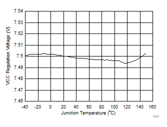 Figure 1. VCC Regulation Voltage vs Junction Temperature
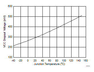
| VIN = 5 V, | IVCC= 20 mA |
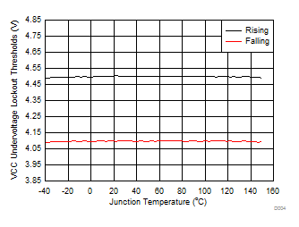 Figure 5. VCC UVLO Threshold vs Junction Temperature
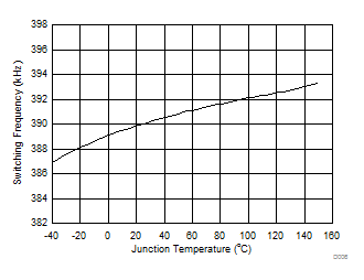
| RT= 20 kΩ |
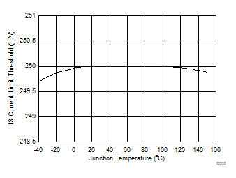 Figure 9. Current Limit Threshold vs Junction Temperature
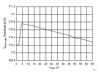
| VIADJ> 2.6 V |
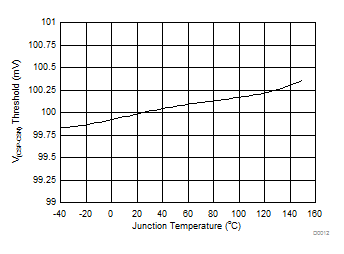
| VIADJ= 1.4 V |
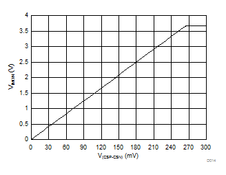 Figure 15. VIMON vs V(CSP-CSN)
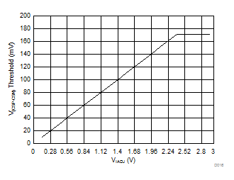 Figure 17. V(CSP-CSN) Threshold vs VIADJ
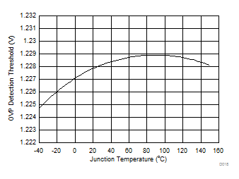 Figure 19. OVP Detection Threshold vs Junction Temperature
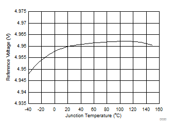 Figure 2. VREF Reference Voltage vs Junction Temperature
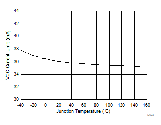 Figure 4. VCC Current Limit vs Junction Temperature
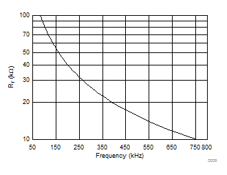 Figure 6. Timing Resistance (RT) vs Switching Frequency
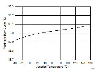 Figure 8. Maximum Duty Cycle vs Junction Temperature
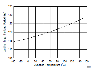 Figure 10. Leading Edge Blanking Period vs Junction Temperature
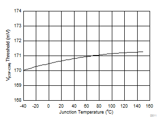
| VIADJ> 2.6 V |
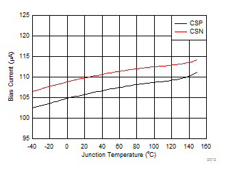
| VCSP= VCSN = 14 V |
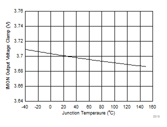 Figure 16. VIMON(CLP) vs Junction Temperature
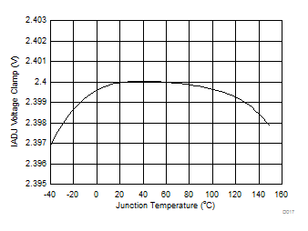 Figure 18. VIADJ Voltage Clamp vs Junction Temperature
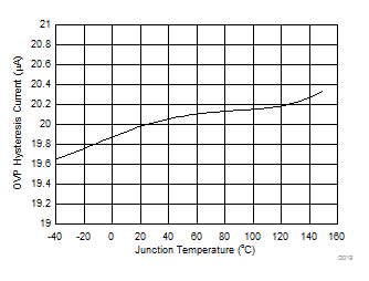 Figure 20. OVP Hysteresis Current vs Junction Temperature