JAJSNY9B September 2022 – February 2023 TPSM365R3 , TPSM365R6
PRODUCTION DATA
- 1 特長
- 2 アプリケーション
- 3 概要
- 4 Revision History
- 5 Description (continued)
- 6 Device Comparison Table
- 7 Pin Configuration and Functions
-
8 Specifications
- 8.1 Absolute Maximum Ratings
- 8.2 ESD Ratings
- 8.3 Recommended Operating Conditions
- 8.4 Thermal Information
- 8.5 Electrical Characteristics
- 8.6 System Characteristics
- 8.7 Typical Characteristics
- 8.8 Typical Characteristics: VIN = 12 V
- 8.9 Typical Characteristics: VIN = 24 V
- 8.10 Typical Characteristics: VIN = 48 V
-
9 Detailed Description
- 9.1 Overview
- 9.2 Functional Block Diagram
- 9.3
Feature Description
- 9.3.1 Input Voltage Range
- 9.3.2 Output Voltage Selection
- 9.3.3 Input Capacitors
- 9.3.4 Output Capacitors
- 9.3.5 Enable, Start-Up, and Shutdown
- 9.3.6 External CLK SYNC (with MODE/SYNC)
- 9.3.7 Switching Frequency (RT)
- 9.3.8 Power-Good Output Operation
- 9.3.9 Internal LDO, VCC UVLO, and BIAS Input
- 9.3.10 Bootstrap Voltage and VBOOT-UVLO (BOOT Terminal)
- 9.3.11 Spread Spectrum
- 9.3.12 Soft Start and Recovery from Dropout
- 9.3.13 Overcurrent Protection (OCP)
- 9.3.14 Thermal Shutdown
- 9.4 Device Functional Modes
-
10Application and Implementation
- 10.1 Application Information
- 10.2
Typical Application
- 10.2.1
600-mA and 300-mA Synchronous Buck Regulator for
Industrial Applications
- 10.2.1.1 Design Requirements
- 10.2.1.2
Detailed Design Procedure
- 10.2.1.2.1 Custom Design With WEBENCH® Tools
- 10.2.1.2.2 Output Voltage Setpoint
- 10.2.1.2.3 Switching Frequency Selection
- 10.2.1.2.4 Input Capacitor Selection
- 10.2.1.2.5 Output Capacitor Selection
- 10.2.1.2.6 VCC
- 10.2.1.2.7 CFF Selection
- 10.2.1.2.8 Power-Good Signal
- 10.2.1.2.9 Maximum Ambient Temperature
- 10.2.1.2.10 Other Connections
- 10.2.1.3 Application Curves
- 10.2.1
600-mA and 300-mA Synchronous Buck Regulator for
Industrial Applications
- 10.3 Power Supply Recommendations
- 10.4 Layout
- 11Device and Documentation Support
- 12Mechanical, Packaging, and Orderable Information
9.3.12.1 Recovery from Dropout
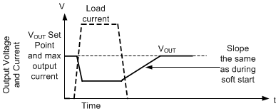
Any time the output voltage falls more than a few percent, output voltage ramps up slowly. This condition, called graceful recovery from dropout in this document, differs from soft start in two important ways:
- The reference voltage is set to approximately 1% above what is needed to achieve the existing output voltage.
- If the device is set to FPWM, it continues to operate in that mode during its recovery from dropout. If output voltage were to suddenly be pulled up by an external supply, the TPSM365Rx can pull down on the output. Note that all protections that are present during normal operation are in place, preventing any catastrophic failure if output is shorted to a high voltage or ground.
 Figure 9-12 Recovery from Dropout
Whether the output voltage falls due to high load or low input voltage, after the condition that causes the output to fall below its set point is removed, the output climbs at the same speed as during start-up. Figure 9-12 shows an example of this behavior.