JAJSEZ8A July   2017  – March 2018 TPSM82480

PRODUCTION DATA.  

  1. 特長
  2. アプリケーション
  3. 概要
    1.     Device Images
      1.      代表的なアプリケーションの回路図 space
      2.      効率と出力電流との関係 space space
  4. 改訂履歴
  5. Pin Configuration and Functions
    1.     Pin Functions
  6. Specifications
    1. 6.1 Absolute Maximum Ratings
    2. 6.2 ESD Ratings
    3. 6.3 Recommended Operating Conditions
    4. 6.4 Thermal Information
    5. 6.5 Electrical Characteristics
    6. 6.6 Typical Characteristics
  7. Detailed Description
    1. 7.1 Overview
    2. 7.2 Functional Block Diagram
    3. 7.3 Feature Description
      1. 7.3.1  Enable / Shutdown (EN)
      2. 7.3.2  Soft Start (SS), Pre-biased Output
      3. 7.3.3  Tracking (TR)
      4. 7.3.4  Output Voltage Select (VSEL)
      5. 7.3.5  Forced PWM (MODE)
      6. 7.3.6  Power Good (PG)
      7. 7.3.7  Thermal Good (TG)
      8. 7.3.8  Active Output Discharge
      9. 7.3.9  Undervoltage Lockout (UVLO)
      10. 7.3.10 Thermal Shutdown
    4. 7.4 Device Functional Modes
      1. 7.4.1 Pulse Width Modulation (PWM) Operation
      2. 7.4.2 Power Save Mode (PSM) Operation
      3. 7.4.3 Minimum Duty Cycle and 100% Mode Operation
      4. 7.4.4 Phase Shifted Operation
      5. 7.4.5 Phase Add/Shed and Current Balancing
      6. 7.4.6 Current Limit and Short Circuit Protection
  8. Application and Implementation
    1. 8.1 Application Information
    2. 8.2 Typical Application
      1. 8.2.1 Design Requirements
      2. 8.2.2 Detailed Design Procedure
        1. 8.2.2.1 Setting the Adjustable Output Voltage
        2. 8.2.2.2 Setting VOUT2 Using the VSEL Feature
        3. 8.2.2.3 Output Capacitor Selection
        4. 8.2.2.4 Input Capacitor Selection
        5. 8.2.2.5 Soft Start Capacitor Selection
        6. 8.2.2.6 Tracking
        7. 8.2.2.7 Thermal Good
      3. 8.2.3 Application Curves
    3. 8.3 System Examples
  9. Power Supply Recommendations
  10. 10Layout
    1. 10.1 Layout Guidelines
    2. 10.2 Layout Example
  11. 11デバイスおよびドキュメントのサポート
    1. 11.1 ドキュメントのサポート
      1. 11.1.1 関連資料
    2. 11.2 ドキュメントの更新通知を受け取る方法
    3. 11.3 コミュニティ・リソース
    4. 11.4 商標
    5. 11.5 静電気放電に関する注意事項
    6. 11.6 Glossary
  12. 12メカニカル、パッケージ、および注文情報

パッケージ・オプション

メカニカル・データ(パッケージ|ピン)
サーマルパッド・メカニカル・データ
発注情報

Pin Configuration and Functions

MOP Package
24-Pin QFM
TPSM82480 SLVSDT1_pinout.gif
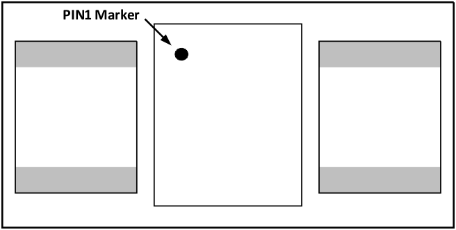
TPSM82480 SLVSDT1_pin1.gifFigure 1. Pin1 Marking on IC


Pin Functions

PIN I/O DESCRIPTION
NAME NO.
VOUT1 1 Output Voltage Node Phase 1 (master), Must be connect with VOUT2
PGND1 2, 3, 20,21 Power Ground Phase 1 (master)
VIN1 4, 24 Supply voltage Phase 1 (master)
EN 5 Enable input (High=Enabled, Low = Disabled)
PG 6 Power Good (open drain, requires pull-up resistor)
VSEL 7 Output Voltage Select (High = VOUT2, Low=VOUT1) , VOUT1 < VOUT2
TG 8 Thermal Good (open drain, requires pull-up resistor)
MODE 9 Operating mode selection (Low=Automatic PWM/PSM, High = Forced PWM)
VIN2 10, 23 Supply voltage Phase 2
PGND2 11,12, 14, 22 Power Ground Phase 2
VOUT2 13 Output Voltage Node Phase 2, Must be connected with VOUT1
SS/TR 15 Soft-Start / Tracking. An external capacitor connected to this pin sets the output voltage rise time.
AGND 16 Analog Ground
FB 17 Output voltage feedback for the adjustable version. Connect resistive voltage divider to this pin.
RS 18 Resistor Select. Connect resistor that sets the level for the second output voltage here (activated by VSEL= High)
VO 19 VOUT detection (connect to VOUT, output discharge is internally connected to this pin)