JAJSQ56 November 2024 TPSM84338
PRODUCTION DATA
- 1
- 1 特長
- 2 アプリケーション
- 3 概要
- 4 Pin Configuration and Functions
- 5 Specifications
-
6 Detailed Description
- 6.1 Overview
- 6.2 Functional Block Diagram
- 6.3
Feature Description
- 6.3.1 Fixed Frequency Peak Current Mode
- 6.3.2 Mode Selection
- 6.3.3 Voltage Reference
- 6.3.4 Output Voltage Setting
- 6.3.5 Switching Frequency Selection, Synchronization
- 6.3.6 Phase Shift
- 6.3.7 Enable and Adjusting Undervoltage Lockout
- 6.3.8 External Soft Start and Prebiased Soft Start
- 6.3.9 Power Good
- 6.3.10 Minimum On Time, Minimum Off Time, and Frequency Foldback
- 6.3.11 Frequency Spread Spectrum
- 6.3.12 Overvoltage Protection
- 6.3.13 Overcurrent and Undervoltage Protection
- 6.3.14 Thermal Shutdown
- 6.4 Device Functional Modes
-
7 Application and Implementation
- 7.1
Typical Application
- 7.1.1 Design Requirements
- 7.1.2
Detailed Design Procedure
- 7.1.2.1 Custom Design With WEBENCH® Tools
- 7.1.2.2 Output Voltage Resistors Selection
- 7.1.2.3 Choosing Switching Frequency
- 7.1.2.4 Soft-Start Capacitor Selection
- 7.1.2.5 Output Capacitor Selection
- 7.1.2.6 Input Capacitor Selection
- 7.1.2.7 Feedforward Capacitor CFF Selection
- 7.1.2.8 Maximum Ambient Temperature
- 7.1.3 Application Curves
- 7.2 Best Design Practices
- 7.3 Power Supply Recommendations
- 7.4 Layout
- 7.1
Typical Application
- 8 Device and Documentation Support
- 9 Revision History
- 10Mechanical, Packaging, and Orderable Information
6.3.1 Fixed Frequency Peak Current Mode
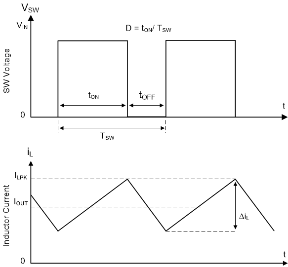
The following operation description of the TPSM84338 refers to the functional block diagram and to the waveforms in Figure 6-1. The TPSM84338 is a synchronous buck converter with integrated high-side (HS) and low-side (LS) MOSFETs (synchronous rectifier). The TPSM84338 supplies a regulated output voltage by turning on the HS and LS NMOS switches with controlled duty cycle. During high-side switch on time, the SW pin voltage swings up to approximately VIN, and the inductor current, iL, increases with linear slope (VIN – VOUT) / L. When the HS switch is turned off by the control logic, the LS switch is turned on after an anti-shoot–through dead time. Inductor current discharges through the low-side switch with a slope of –VOUT / L. The control parameter of a buck converter is defined as Duty Cycle D = tON / tSW, where tON is the high-side switch on time and tSW is the switching period. The converter control loop maintains a constant output voltage by adjusting the duty cycle D. In an ideal buck converter where losses are ignored, D is proportional to the output voltage and inversely proportional to the input voltage: D = VOUT / VIN.
 Figure 6-1 SW Node and Inductor Current Waveforms in Continuous Conduction Mode
(CCM)
Figure 6-1 SW Node and Inductor Current Waveforms in Continuous Conduction Mode
(CCM)The TPSM84338 employs the fixed-frequency peak current mode control. A voltage feedback loop is used to get accurate DC voltage regulation by adjusting the peak current command based on voltage offset. The peak inductor current is sensed from the HS switch and compared to the peak current threshold to control the on time of the HS switch. The voltage feedback loop is internally compensated, which allows for fewer external components, makes design easy, and provides stable operation with almost any combination of output capacitors.