JAJSC61C May 2016 – May 2016 TRS3122E
PRODUCTION DATA.
- 1 特長
- 2 アプリケーション
- 3 概要
- 4 改訂履歴
- 5 Pin Configuration and Functions
-
6 Specifications
- 6.1 Absolute Maximum Ratings
- 6.2 ESD Ratings
- 6.3 Recommended Operating Conditions
- 6.4 Thermal Characteristics
- 6.5 Power and Status Electrical Characteristics
- 6.6 Driver Electrical Characteristics
- 6.7 Receiver Electrical Characteristics
- 6.8 Driver Switching Characteristics
- 6.9 Receiver Switching Characteristics
- 6.10 Power and Status Switching Characteristics
- 6.11 Typical Characteristics
- 7 Parameter Measurement Information
- 8 Detailed Description
- 9 Application and Implementation
- 10Power Supply Recommendations
- 11Layout
- 12デバイスおよびドキュメントのサポート
- 13メカニカル、パッケージ、および注文情報
9 Application and Implementation
NOTE
Information in the following applications sections is not part of the TI component specification, and TI does not warrant its accuracy or completeness. TI’s customers are responsible for determining suitability of components for their purposes. Customers should validate and test their design implementation to confirm system functionality.
9.1 Application Information
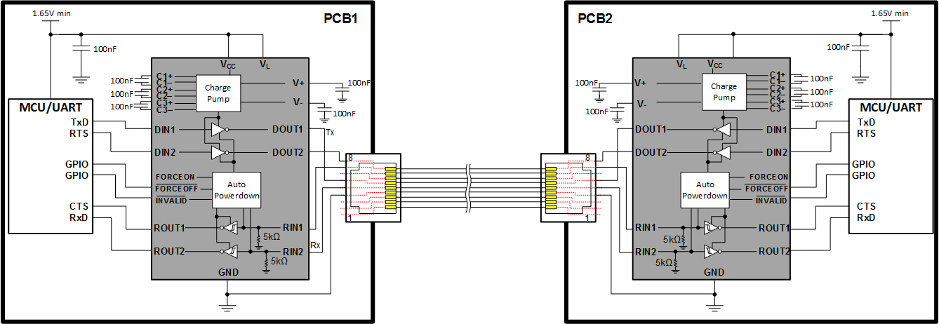
RS232 is used to communicate between two electrical units on separate PCBs across cables <40 ft. Common RS232 cables are RJ45, DB9 & DB25.
9.2 Typical 1.8-V Application
 Figure 13. TRS3122E Typical Application
9.2.1 Design Requirements
For this design example, use the parameters listed in Table 2 as the input parameters.
Table 2. Design Parameters
| DESIGN PARAMETER | EXAMPLE VALUE |
|---|---|
| MCU GPIO Supple Voltage | 1.8 V |
| Transmission Voltage | +/-4.7 V |
| Data-rate | 1 Mbps |
| Number of Transmitters / Receivers | 2 |
| Charge Pump Capacitor Values | 100nF (see Table 3) |
9.2.2 Detailed Design Procedure
When using TRS3122E, determine the following:
- All DIN, FORCEOFF, and FORCEON inputs must be connected to valid low or high logic levels.
- Select capacitor values based on VCC level for best performance. (see Table 3)
9.2.2.1 Data-Rate and Cable Length
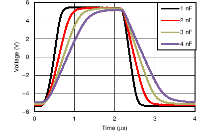
RS-232 intended is for short range data transmission. The rise time for RS-232 driver edges is slow enough that the data cable appears as a capacitor instead of a transmission line impedance. The elapsed time for one bit of data far exceeds the transit time of any practical RS-232 cable length. The capacitance of the cable is the limiting factor. Therefore the capacitance per foot (or meter) of the cable is important if long data cables are used. Capacitance slows the rise and fall time of the signal. For low data rates, the delay is insignificant. However, high data rates will have reduced percentage of time that the output is at VOL or VOH and more time in the transitions. The timing of the UART (universal asynchronous receiver/transmitter) must sample the signal at the right time to coincide with VOL and VOH plateaus. At some point data reliability will be impacted. There are no hard limits for cable capacitance and data rate.
 Figure 14. Typical Waveform with Capacitive Load
VCC = 3.3 V, RLOAD = 3 kΩ, Date Rate = 500kbps
The maximum cable length depends on the cable used (pf/ft), data rate, timing of receiving UART, system tolerance to data errors.
9.2.2.2 Capacitor Selection
The capacitor type used for C1–C5 is not critical for proper operation; polarized or non-polarized capacitors can be used, though lower ESR capacitors are preferred. The charge pump requires 0.1 μF capacitors for VCC = 1.8-V or VCC = 3.3-V operation. For other supply voltages, see Table 1 for required capacitor values. Do not use values smaller than those listed in Table 1. Increasing the capacitor values(e.g., by a factor of 2), except for C1, reduces ripple on the transmitter outputs and slightly reduces power consumption. C2, C3, C4 and C5 can be increased without changing C1’s value. However, do not increase C1 without also increasing the values of C2, C3, C4, C5, CBYPASS1, and CBYPASS2 to maintain the proper ratios (C1 to the other capacitors). When using the minimum required capacitor values, make sure the capacitor value does not degrade excessively with temperature. If in doubt, use capacitors with a larger nominal value. The capacitor’s equivalent series resistance (ESR) usually increases at low temperatures.
For best charge pump efficiency locate the charge pump and bypass capacitors as close as possible to the IC. Surface mount capacitors are best for this purpose. Using capacitors with lower equivalent series resistance (ESR) and self-inductance, along with minimizing parasitic PCB trace inductance will optimize charge pump operation. Designers are also advised to consider that capacitor values may shift over time and operating temperature.
Table 3. Capacitor Selection
| VCC = VL | C1 Capacitor Value | C2 Capacitor Value | C3 Capacitor Value | C4 Capacitor Value | C5 Capacitor Value |
|---|---|---|---|---|---|
| 1.65 V to 2 V(1) | 100 nF | ||||
| 3.0 V to 3.6 V(1) | 100 nF | 100 nF or open | 100 nF | ||
| 4.5 V to 5.5 V(1) | 47 nF | 330 nF | 100 nF or open | 330 nF | |
| 3 V to 5.5 V(2) | 47 nF | 470 nF | 100 nF or open | 470 nF | |
