JAJSLZ3C July 2007 – December 2024 TRSF3221E
PRODUCTION DATA
- 1
- 1 特長
- 2 アプリケーション
- 3 概要
- 4 Pin Configuration and Functions
-
5 Specifications
- 5.1 Absolute Maximum Ratings
- 5.2 ESD Ratings
- 5.3 ESD Ratings, IEC Specifications
- 5.4 Recommended Operating Conditions
- 5.5 Thermal Resistance Characteristics
- 5.6 Electrical Characteristics
- 5.7 Electrical Characteristics, Driver
- 5.8 Switching Characteristics, Driver
- 5.9 Electrical Characteristics, Receiver
- 5.10 Switching Characteristics, Receiver
- 5.11 Electrical Characteristics, Auto-Powerdown
- 5.12 Switching Characteristics, Auto-Powerdown
- 5.13 Typical Characteristics
- 6 Parameter Measurement Information
- 7 Detailed Description
- 8 Application and Implementation
- 9 Device and Documentation Support
- 10Revision History
- 11Mechanical, Packaging, and Orderable Information
パッケージ・オプション
メカニカル・データ(パッケージ|ピン)
サーマルパッド・メカニカル・データ
- RGT|16
発注情報
8.1.1 Typical Application
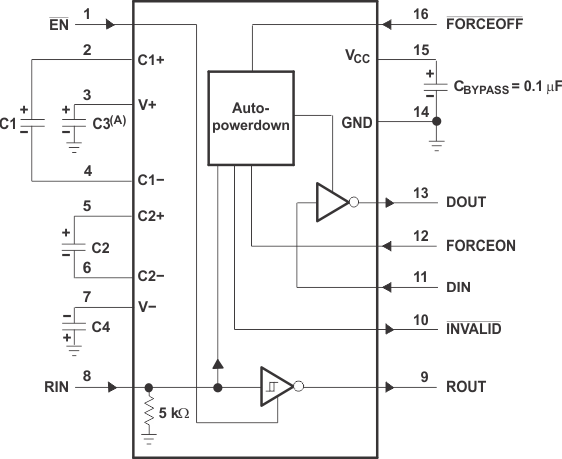
ROUT and DIN connect to UART or general purpose logic lines. FORCEON and FORCEOFFmay be connected general purpose logic lines or tied to ground or VCC. INVALID may be connected to a general purpose logic line or left unconnected. RIN and DOUT lines connect to a RS-232 connector or cable. DIN, FORCEON, and FORCEOFF inputs must not be left unconnected.

| VCC | C1 | C2, C3, C4 | ||
|---|---|---|---|---|
| 3.3V ± 0.3V | 0.1µF | 0.1µF | ||
| 5V ± 0.5V | 0.047µF | 0.33µF | ||
| 3V to 5.5V | 0.1µF | 0.47µF | ||