-
TS12A4451x Low ON-State Resistance 4-Channel SPST CMOS Analog Switches SCDS247B October 2008 – February 2016 TS12A44513 , TS12A44514 , TS12A44515
PRODUCTION DATA.
-
TS12A4451x Low ON-State Resistance 4-Channel SPST CMOS Analog Switches
- 1 Features
- 2 Applications
- 3 Description
- 4 Revision History
- 5 Pin Configuration and Functions
- 6 Specifications
- 7 Detailed Description
- 8 Application and Implementation
- 9 Power Supply Recommendations
- 10Layout
- 11Device and Documentation Support
- 12Mechanical, Packaging, and Orderable Information
- IMPORTANT NOTICE
パッケージ・オプション
メカニカル・データ(パッケージ|ピン)
サーマルパッド・メカニカル・データ
発注情報
TS12A4451x Low ON-State Resistance 4-Channel SPST CMOS Analog Switches
1 Features
- 2-V to 12-V Single-Supply Operation
- Specified ON-State Resistance:
- 15-Ω Maximum With 12-V Supply
- 20-Ω Maximum With 5-V Supply
- 50-Ω Maximum With 3.3-V Supply
- ΔRON Matching
- 2.5-Ω (Max) at 12 V
- 3-Ω (Max) at 5 V
- 3.5-Ω (Max) at 3.3 V
- Specified Low OFF-Leakage Currents:
- 1 nA at 25°C
- 10 nA at 85°C
- Specified Low ON-Leakage Currents:
- 1 nA at 25°C
- 10 nA at 85°C
- Low Charge Injection: 11.5 pC (12-V Supply)
- Fast Switching Speed:
tON = 80 ns, tOFF = 50 ns (12-V Supply) - Break-Before-Make Operation (tON > tOFF)
- TTL/CMOS-Logic Compatible With 5-V Supply
- Available in 14-Pin TSSOP Package or 14-Pin SOIC Package
2 Applications
- Data Acquisition Systems
- Communication Circuits
- Signal Routing
- Computer Peripherals
3 Description
The TS12A44513, TS12A44514, and TS12A44515 devices have four bidirectional single-pole single-throw (SPST) single-supply CMOS analog switches. The TS12A44513 has two normally closed (NC) switches and two normally open (NO) switches, the TS12A44514 has four NO switches, and the TS12A44515 has four NC switches.
These CMOS switches may operate continuously with a single supply from 2 V to 12 V and can handle rail-to-rail analog signals. The OFF-leakage current maximum is only 1 nA at 25°C or 10 nA at 85°C.
When using a 5-V supply, all digital inputs have 0.8-V to 2.4-V logic thresholds, ensuring TTL/CMOS-logic compatibility.
Device Information(1)
| PART NUMBER | PACKAGE | BODY SIZE (NOM) |
|---|---|---|
| TS12A44513, TS12A44514, TS12A44515 | TSSOP (14) | 5.00 mm x 4.4 mm |
| SOIC (14) | 8.65 mm x 3.91 mm |
- For all available packages, see the orderable addendum at the end of the datasheet.
Simplified Schematic

4 Revision History
Changes from A Revision (November 2014) to B Revision
- Changed VCC min value from 0 to 2 in Recommended Operating Conditions tableGo
- Added Supply column back into all Electrical Characteristics tablesGo
Changes from * Revision (October 2008) to A Revision
- Added Pin Configuration and Functions section, ESD Ratings table, Feature Description section, Device Functional Modes, Application and Implementation section, Power Supply Recommendations section, Layout section, Device and Documentation Support section, and Mechanical, Packaging, and Orderable Information section Go
5 Pin Configuration and Functions

Pin Functions
| PIN | I/O | DESCRIPTION | |||
|---|---|---|---|---|---|
| NAME | TS12A44513 | TS12A44514 | TS12A44515 | ||
| COM | 2, 4, 9, 10 | 2, 4, 9, 10 | 2, 4, 9, 10 | I/O | Common |
| VCC | 14 | 14 | 14 | I | Power supply |
| IN | 5, 6, 12, 13 | 5, 6, 12, 13 | 5, 6, 12, 13 | I | Digital control to connect COM to NO or NC |
| GND | 7 | 7 | 7 | GND | Ground |
| NO | 1, 8 | 1, 3, 8, 11 | – | I/O | Normally open |
| NC | 3, 11 | – | 1, 3, 8, 11 | I/O | Normally closed |
6 Specifications
6.1 Absolute Maximum Ratings(1)(2)(3)
| MIN | MAX | UNIT | ||||
|---|---|---|---|---|---|---|
| VCC | Supply voltage | –0.3 | 13 | V | ||
| VNC
VNO VCOM |
Analog voltage(4) | –0.3 | VCC + 0.3 | V | ||
| INC
INO ICOM IIN |
Analog current | -20 | 20 | mA | ||
| Peak current (pulsed at 1 ms, 10% duty cycle) | ±30 | mA | ||||
| TA | Operating temperature | –40 | 85 | °C | ||
| PD | Power dissipation | Mounted on JEDEC 4-layer board (JESD 51-7), No airflow, TA = 25°C, TJ = 125°C | PW package | 0.88 | W | |
| Tstg | Storage temperature | –65 | 150 | °C | ||
6.2 ESD Ratings
| VALUE | UNIT | |||
|---|---|---|---|---|
| V(ESD) | Electrostatic discharge | Human-body model (HBM), per ANSI/ESDA/JEDEC JS-001(1) | ±2000 | V |
| Charged-device model (CDM), per JEDEC specification JESD22-C101(2) | ±500 | |||
6.3 Recommended Operating Conditions
over operating free-air temperature range (unless otherwise noted)| MIN | MAX | UNIT | ||
|---|---|---|---|---|
| VCC | 2 | 12 | V | |
| VNC, VNO, VCOM, VIN | 0 | VCC | V | |
6.4 Thermal Information
| THERMAL METRIC(1) | TS12A44513, TS12A44514, TS12A44515 | UNIT | ||
|---|---|---|---|---|
| D | PW | |||
| 14 PINS | 14 PINS | |||
| RθJA | Junction-to-ambient thermal resistance | 89.8 | 119.6 | °C/W |
| RθJC(top) | Junction-to-case (top) thermal resistance | 49.6 | 48.4 | |
| RθJB | Junction-to-board thermal resistance | 44.4 | 61.3 | |
| ψJT | Junction-to-top characterization parameter | 13.8 | 5.7 | |
| ψJB | Junction-to-board characterization parameter | 44.1 | 60.7 | |
6.5 Electrical Characteristics for 5-V Supply(1)
VCC = 4.5 V to 5.5 V, VINH = 2.4 V, VINL = 0.8 V, TA = –40°C to 85°C (unless otherwise noted)| PARAMETER | TEST CONDITIONS | TA | MIN | TYP(2) | MAX | UNIT | ||
|---|---|---|---|---|---|---|---|---|
| ANALOG SWITCH | ||||||||
| VCOM, VNO, VNC | Analog signal range | 0 | VCC | V | ||||
| Ron | ON-state resistance | VCC = 4.5 V, VCOM = 3.5 V, ICOM = 1 mA |
25°C | 12 | 20 | Ω | ||
| Full | 30 | |||||||
| Ron(flat) | ON-state resistance flatness |
VCOM = 1 V, 2 V, 3 V, ICOM = 1 mA |
25°C | 1 | 3 | Ω | ||
| Full | 4 | |||||||
| ΔRon | ON-state resistance matching between channels(5) |
VCC = 4.5 V, ICOM = 5 mA, VNO or VNC = 3 V |
25°C | 3 | Ω | |||
| TMIN to TMAX | 4 | |||||||
| INO(OFF),
INC(OFF) |
NO, NC OFF leakage current(3) |
VCC = 5.5 V, VCOM = 1 V, VNO or VNC = 4.5 V |
25°C | 1 | nA | |||
| Full | 10 | |||||||
| ICOM(OFF) | COM OFF leakage current(3) |
VCC = 5.5 V, VCOM = 1 V, VNO or VNC = 4.5 V |
25°C | 1 | nA | |||
| Full | 10 | |||||||
| ICOM(ON) | COM ON leakage current(3) |
VCC = 5.5 V, VCOM = 4.5 V, VNO or VNC = 4.5 V |
25°C | 1 | nA | |||
| Full | 10 | |||||||
| DIGITAL CONTROL INPUT (IN) | ||||||||
| VIH | Input logic high | Full | 2.4 | VCC | V | |||
| VIL | Input logic low | Full | 0 | 0.8 | V | |||
| IIH, IIL | Input leakage current | VIN = VCC, 0 V | Full | 0.01 | μA | |||
| DYNAMIC | ||||||||
| tON | Turn-on time | see Figure 2 | 25°C | 45 | 100 | ns | ||
| Full | 125 | |||||||
| tOFF | Turn-off time | see Figure 2 | 25°C | 35 | 50 | ns | ||
| Full | 70 | |||||||
| QC | Charge injection(4) | CL = 1 nF, VNO = 0 V, RS = 0 Ω, See Figure 1 |
25°C | –1.5 | pC | |||
| CNO(OFF), CNC(OFF) |
NO, NC OFF capacitance |
f = 1 MHz, See Figure 4 | 25°C | 8 | pF | |||
| CCOM(OFF) | COM OFF capacitance |
f = 1 MHz, See Figure 4 | 25°C | 8 | pF | |||
| CCOM(ON) | COM ON capacitance |
f = 1 MHz, See Figure 4 | 25°C | 19 | pF | |||
| CI | Digital input capacitance | VIN = VCC, 0 V | 25°C | 2 | pF | |||
| BW | Bandwidth | RL = 50 Ω, CL = 15 pF, VNO = 1 VRMS, |
25°C | 530 | MHz | |||
| OISO | OFF isolation | RL = 50 Ω, CL = 15 pF, VNO = 1 VRMS, f = 100 kHz |
25°C | –94 | dB | |||
| THD | Total harmonic distortion | RL = 50 Ω, CL = 15 pF, VNO = 1 VRMS, f = 100 kHz |
25°C | 0.09% | ||||
| SUPPLY | ||||||||
| ICC | Supply Current | VIN = VCC, 0 V | 25°C | 0.05 | μA | |||
| Full | 0.1 | |||||||
6.6 Electrical Characteristics for 12-V Supply(1)
VCC = 11.4 V to 12.6 V, VINH = 5 V, VINL = 0.8 V, TA = –40°C to 85°C (unless otherwise noted)| PARAMETER | TEST CONDITIONS | TA | MIN | TYP(2) | MAX | UNIT | ||
|---|---|---|---|---|---|---|---|---|
| ANALOG SWITCH | ||||||||
| VCOM, VNO, VNC | Analog signal range | 0 | VCC | V | ||||
| Ron | ON-state resistance | VCC = 11.4 V, VCOM = 10 V, ICOM = 1 mA |
25°C | 6.5 | 10 | Ω | ||
| Full | 15 | |||||||
| Ron(flat) | ON-state resistance flatness |
VCC = 11.4 V, VCOM = 2 V, 5 V, 10 V, ICOM = 1 mA |
25°C | 1.5 | 3 | Ω | ||
| Full | 4 | |||||||
| ΔRon | ON-state resistance matching between channels(5) |
VCC = 11.4 V, ICOM = 5 mA, VNO or VNC = 10 V |
25°C | 2.5 | Ω | |||
| TMIN to TMAX | 3 | |||||||
| INO(OFF),
INC(OFF) |
NO, NC OFF leakage current(3) |
VCC = 12.6 V, VCOM = 1 V, VNO or VNC = 10 V |
25°C | 1 | nA | |||
| Full | 10 | |||||||
| ICOM(OFF) | COM OFF leakage current(3) |
VCC = 12.6 V, VCOM = 1 V, VNO or VNC = 10 V |
25°C | 1 | nA | |||
| Full | 10 | |||||||
| ICOM(ON) | COM ON leakage current(3) |
VCC = 12.6 V, VCOM = 10 V, VNO or VNC = 10 V |
25°C | 1 | nA | |||
| Full | 10 | |||||||
| DIGITAL CONTROL INPUT (IN) | ||||||||
| VIH | Input logic high | Full | 5 | VCC | V | |||
| VIL | Input logic low | Full | 0 | 0.8 | V | |||
| IIH, IIL | Input leakage current | VIN = VCC, 0 V | Full | 0.001 | μA | |||
| DYNAMIC | ||||||||
| tON | Turn-on time | See Figure 2 | 25°C | 25 | 75 | ns | ||
| Full | 80 | |||||||
| tOFF | Turn-off time | See Figure 2 | 25°C | 20 | 45 | ns | ||
| Full | 50 | |||||||
| QC | Charge injection(4) | CL = 1 nF, VNO = 0 V, RS = 0 Ω, See Figure 1 |
25°C | –10.5 | pC | |||
| CNO(OFF), CNC(OFF) |
NO, NC OFF capacitance |
f = 1 MHz, See Figure 4 | 25°C | 8 | pF | |||
| CCOM(OFF) | COM OFF capacitance |
f = 1 MHz, See Figure 4 | 25°C | 8 | pF | |||
| CCOM(ON) | COM ON capacitance |
f = 1 MHz, See Figure 4 | 25°C | 21.5 | pF | |||
| CI | Digital input capacitance | VIN = VCC, 0 V | 25°C | 2 | pF | |||
| BW | Bandwidth | RL = 50 Ω, CL = 15 pF, VNO = 1 VRMS, |
25°C | 530 | MHz | |||
| OISO | OFF isolation | RL = 50 Ω, CL = 15 pF, VNO = 1 VRMS, f = 100 kHz |
25°C | –95 | dB | |||
| THD | Total harmonic distortion | RL = 50 Ω, CL = 15 pF, VNO = 1 VRMS, f = 100 kHz |
25°C | 0.07% | ||||
| SUPPLY | ||||||||
| ICC | Supply Current | VIN = VCC, 0 V | 25°C | 0.05 | μA | |||
| Full | 0.2 | |||||||
6.7 Electrical Characteristics for 3-V Supply(1)
VCC = 3 V to 3.6 V, TA = –40°C to 85°C (unless otherwise noted)| PARAMETER | TEST CONDITIONS | TA | MIN | TYP(2) | MAX | UNIT | ||
|---|---|---|---|---|---|---|---|---|
| ANALOG SWITCH | ||||||||
| VCOM, VNO, VNC | Analog signal range | 0 | VCC | V | ||||
| Ron | ON-state resistance | VCC = 3 V, VCOM = 1.5 V, INO = 1 mA, |
25°C | 20 | 40 | Ω | ||
| Full | 50 | |||||||
| Ron(flat) | ON-state resistance flatness |
VCC = 3 V, VCOM = 1 V, 1.5 V, 2 V, ICOM = 1 mA |
25 °C | 1 | 3 | Ω | ||
| Full | 4 | |||||||
| ΔRon | ON-state resistance matching between channels(5) |
VCC = 2.7 V, ICOM = 5 mA, VNO or VNC = 1.5 V |
25°C | 3.5 | Ω | |||
| TMIN to TMAX | 4.5 | |||||||
| INO(OFF),
INC(OFF) |
NO, NC OFF leakage current(3) |
VCC = 3.6 V, VCOM = 1 V, VNO or VNC = 3 V |
25°C | 1 | nA | |||
| Full | 10 | |||||||
| ICOM(OFF) | COM OFF leakage current(3) |
VCC = 3.6 V, VCOM = 1 V, VNO or VNC = 3 V |
25°C | 1 | nA | |||
| Full | 10 | |||||||
| ICOM(ON) | COM ON leakage current(3) |
VCC = 3.6 V, VCOM = 3 V, VNO or VNC = 3 V |
25°C | 1 | nA | |||
| Full | 10 | |||||||
| DIGITAL CONTROL INPUT (IN) | ||||||||
| VIH | Input logic high | Full | 2.4 | VCC | V | |||
| VIL | Input logic low | Full | 0 | 0.8 | V | |||
| IIH, IIL | Input leakage current | VIN = VCC, 0 V | Full | 0.01 | μA | |||
| DYNAMIC | ||||||||
| tON | Turn-on time(4) | See Figure 2 | 25°C | 70 | 120 | ns | ||
| Full | 175 | |||||||
| tOFF | Turn-off time(4) | See Figure 2 | 25°C | 50 | 80 | ns | ||
| Full | 120 | |||||||
| QC | Charge injection(4) | CL = 1 nF, See Figure 1 | 25°C | –0.5 | pC | |||
| CNO(OFF), CNC(OFF) |
NO, NC OFF capacitance |
f = 1 MHz, See Figure 4 | 25°C | 8 | pF | |||
| CCOM(OFF) | COM OFF capacitance |
f = 1 MHz, See Figure 4 | 25°C | 8 | pF | |||
| CCOM(ON) | COM ON capacitance |
f = 1 MHz, See Figure 4 | 25°C | 17 | pF | |||
| CI | Digital input capacitance | VIN = VCC, 0 V | 25°C | 2 | pF | |||
| BW | Bandwidth | RL = 50 Ω, CL = 15 pF, VNO = 1 VRMS, f = 100 kHz |
25°C | 510 | MHz | |||
| OISO | OFF isolation | RL = 50 Ω, CL = 15 pF, VNO = 1 VRMS, f = 100 kHz |
25°C | –94 | dB | |||
| THD | Total harmonic distortion | RL = 50 Ω, CL = 15 pF, VNO = 1 VRMS, f = 100 kHz |
25°C | 0.27% | ||||
| SUPPLY | ||||||||
| ICC | Supply Current | VIN = VCC, 0 V | 25°C | 0.05 | μA | |||
| Full | 0.2 | |||||||
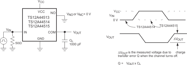 Figure 1. Charge Injection
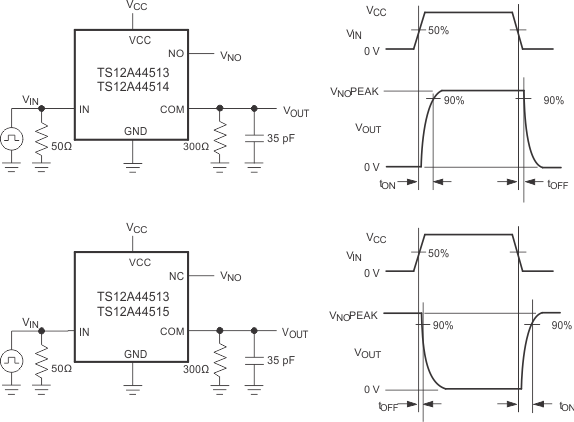 Figure 2. Switching Times
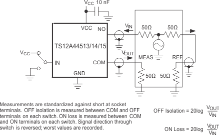 Figure 3. Off Isolation and On Loss
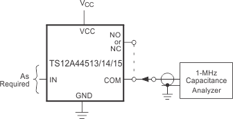 Figure 4. NO, NC, and COM Capacitance
6.8 Typical Characteristics
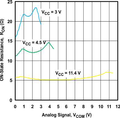 Figure 5. RON vs VCOM (TA = 25°C)
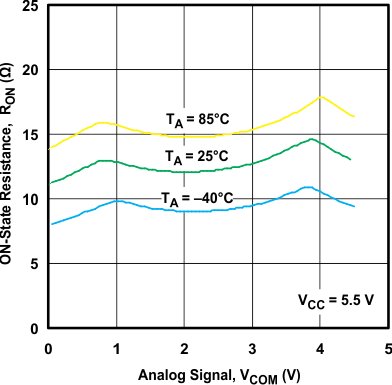 Figure 7. RON vs VCOM (VCC = 4.5 V)
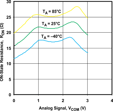 Figure 6. RON vs VCOM (VCC = 3 V)
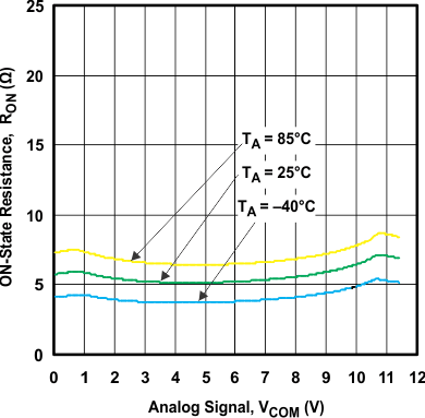 Figure 8. RON vs VCOM (VCC = 11.4 V)
7 Detailed Description
7.1 Overview
The TS12A4451x has 4 bidirectional single-pole single-throw (SPST) single-supply CMOS analog switches. The TS12A44513 has two normally closed (NC) switches and two normally open (NO) switches, the TS12A44514 has four normally open (NO) switches, and the TS12A44515 has four normally closed (NC) switches .
These CMOS switches can operate continuously with a single supply between 2 V and 12 V and can handle rail-to-rail analog signals. The OFF-leakage current maximum is only 1 nA at 25°C or 10 nA at 85°C.
When using a 5-V supply, all digital inputs have 0.8-V to 2.4-V logic thresholds, ensuring TTL/CMOS-logic compatibility.
7.2 Functional Block Diagram

7.3 Feature Description
The TS12A4451x is bidirectional with fast switching times in the 10's of ns range which allows data acquisition and communication between multiple devices.
With a 5-V supply these devices are compatible with standard 1.8-V TTL/CMOS logic.
7.4 Device Functional Modes
Table 1. Function Table
| IN | NO TO COM, COM TO NO | NC TO COM, COM TO NC |
|---|---|---|
| L | OFF | ON |
| H | ON | OFF |