JAJSM20A December 2020 – May 2021 TS3DV642-Q1
PRODUCTION DATA
- 1 特長
- 2 アプリケーション
- 3 概要
- 4 Revision History
- 5 Pin Configuration and Functions
- 6 Specifications
- 7 Parameter Measurement Information
- 8 Detailed Description
- 9 Application and Implementation
- 10Power Supply Recommendations
- 11Layout
- 12Device and Documentation Support
- 13Mechanical, Packaging, and Orderable Information
パッケージ・オプション
デバイスごとのパッケージ図は、PDF版データシートをご参照ください。
メカニカル・データ(パッケージ|ピン)
- RUA|42
サーマルパッド・メカニカル・データ
発注情報
6.8 Typical Characteristics
#FIG_JGQ_RRH_RPB, #FIG_L3V_5RH_RPB, #FIG_SJR_WRH_RPB and #FIG_C5C_ZRH_RPB show typical high speed performance plots for TS3DV642-Q1 in TI evaluation board with measurement parasitics calibrated out.
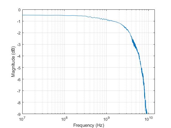 Figure 6-1 Typical
differential gain vs frequency
 |
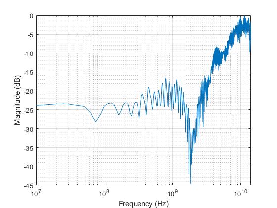 Figure 6-2 Typical
return loss vs frequency
 |
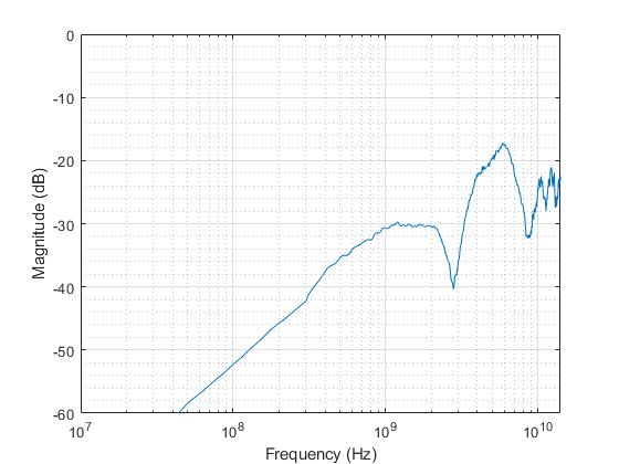 Figure 6-3 Typical
differential cross-talk vs frequency
 |
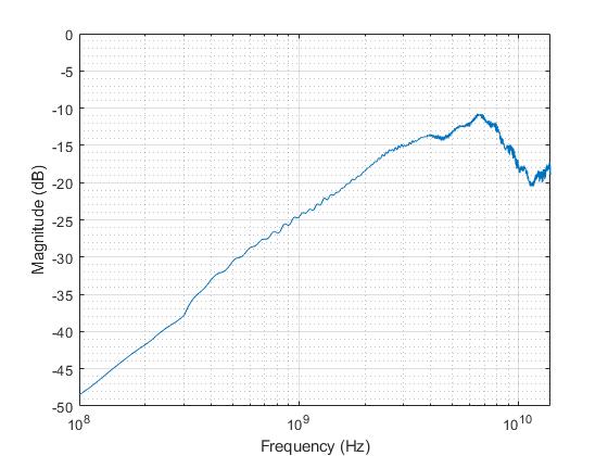 Figure 6-4 Typical
differential off-isolation vs frequency
 |
#FIG_UF4_B54_KPB illustrates eye diagrams at 3.4 Gbps with jitter decomposion shown. As illustrated added total jitter contribution by the TS3DV642-Q1 is minimal - 17 ps and 16 ps through the TS3DV642-Q1 Port A and Port B respectively versus 13 ps through baseline calibration setup without a DUT.


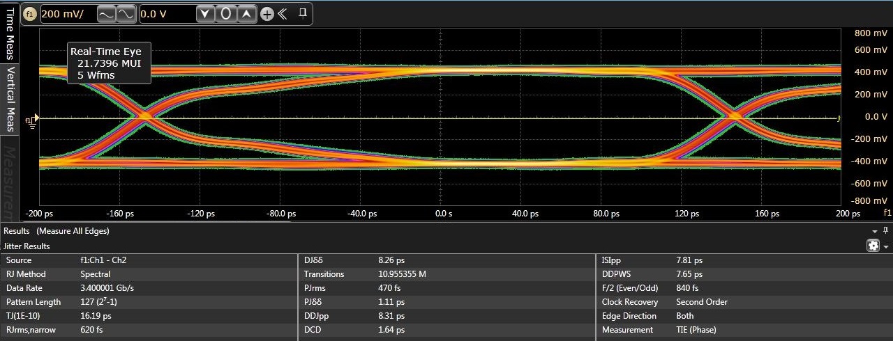 Figure 6-5 Typical eye diagrams at 3.4
Gbps. Top: baseline calibration setup. Middle: through TS3DV642-Q1 Port A.
Bottom: through TS3DV642-Q1 Port B.
Figure 6-5 Typical eye diagrams at 3.4
Gbps. Top: baseline calibration setup. Middle: through TS3DV642-Q1 Port A.
Bottom: through TS3DV642-Q1 Port B.#FIG_TB3_53L_LPB illustrates eye diagrams at 6.0 Gbps with jitter decomposition shown. As illustrated added total jitter contribution by the TS3DV642-Q1 is minimal - 20 ps and 17 ps through the TS3DV642-Q1 Port A and Port B respectively versus 12 ps through baseline calibration setup without a DUT.

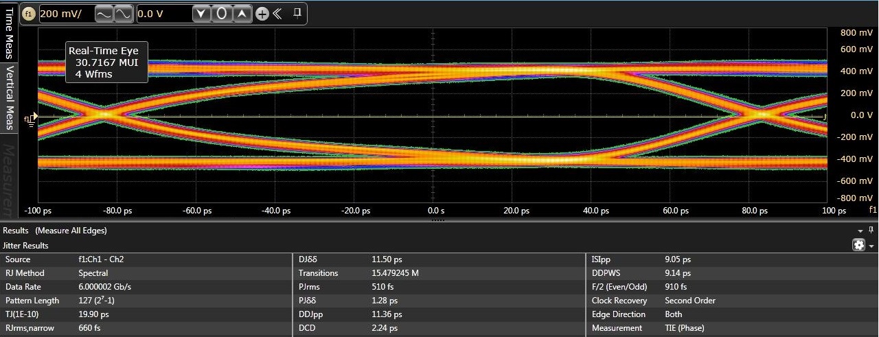
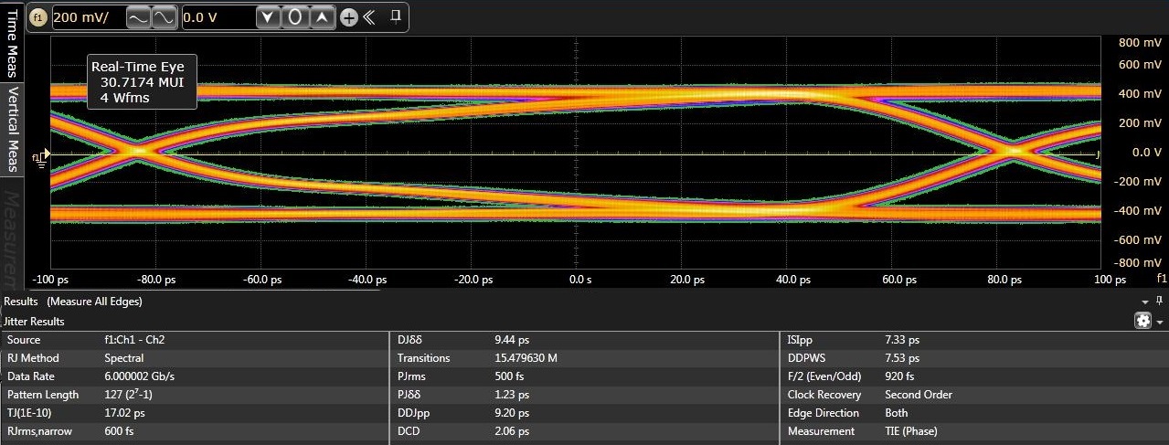 Figure 6-6 Typical eye diagrams at 6.0
Gbps. Top: baseline calibration setup. Middle: through TS3DV642-Q1 Port A.
Bottom: through TS3DV642-Q1 Port B.