JAJSP87D September 2010 – October 2022 TS3L501E
PRODUCTION DATA
- 1 特長
- 2 アプリケーション
- 3 概要
- 4 Revision History
- 5 Pin Configuration and Functions
-
6 Specifications
- 6.1 Absolute Maximum Ratings
- 6.2 ESD Ratings
- 6.3 Recommended Operating Conditions
- 6.4 Thermal Information
- 6.5 Electrical Characteristics for 1000 Base-T Ethernet Switching
- 6.6 Electrical Characteristics for 10/100 Base-T Ethernet Switching
- 6.7 Switching Characteristics
- 6.8 Dynamic Characteristics
- 6.9 Typical Characteristics
- 7 Parameter Measurement Information
- 8 Detailed Description
- 9 Application and Implementation
- 10Power Supply Recommendations
- 11Layout
- 12Device and Documentation Support
- 13Mechanical, Packaging, and Orderable Information
パッケージ・オプション
メカニカル・データ(パッケージ|ピン)
- RUA|42
サーマルパッド・メカニカル・データ
- RUA|42
発注情報
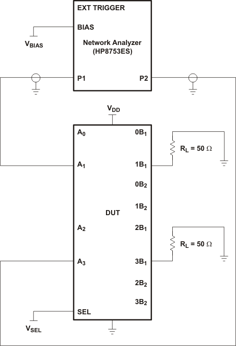
7.3 HP8753ES Setup
Average = 4
RBW = 3 kHz
VBIAS = 0.35 V
ST = 2 s
P1 = 0 dBM

A. CL includes probe and jig capacitance.
B. A 50-Ω termination resistor is needed to match the loading of the network analyzer.
Figure 7-4 Test Circuit for Crosstalk (XTALK)Crosstalk is measured at the output of the nonadjacent ON channel. For example, when VSEL = 0 and A1 is the input, the output is measured at A3. All unused analog input (A) ports are connected to GND, and output (B) ports are left open.