SCDS241B May 2008 – December 2016 TS5A9411
PRODUCTION DATA.
- 1 Features
- 2 Applications
- 3 Description
- 4 Revision History
- 5 Pin Configuration and Functions
- 6 Specifications
- 7 Parameter Measurement Information
- 8 Detailed Description
- 9 Application and Implementation
- 10Power Supply Recommendations
- 11Layout
- 12Device and Documentation Support
- 13Mechanical, Packaging, and Orderable Information
9 Application and Implementation
NOTE
Information in the following applications sections is not part of the TI component specification, and TI does not warrant its accuracy or completeness. TI’s customers are responsible for determining suitability of components for their purposes. Customers should validate and test their design implementation to confirm system functionality.
9.1 Application Information
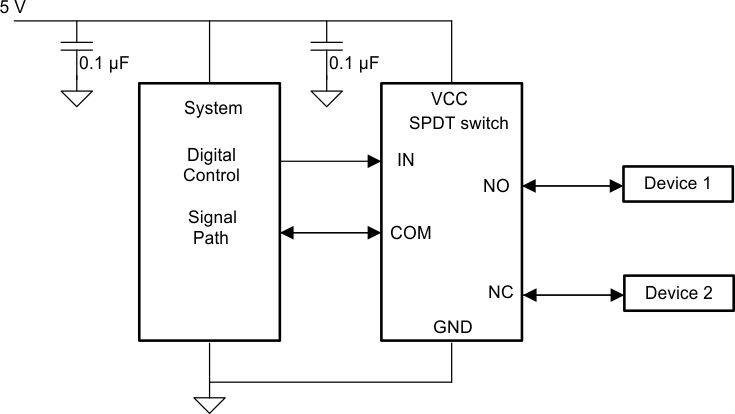
The switches are bidirectional, so the NO, NC, and COM pins can be used as either inputs or outputs. The device is used in systems where multiple analog or digital signals must be selected to pass across a single line.
9.2 Typical Application
 Figure 16. Typical Application Diagram
9.2.1 Design Requirements
Pull the digitally controlled input select pin (IN) to VCC or GND to avoid unwanted switch states that could result if the logic control pin is left floating.
9.2.2 Detailed Design Procedure
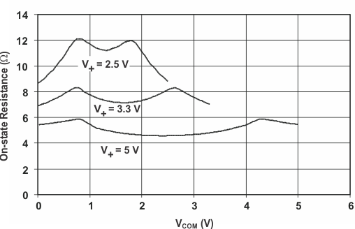
Select the appropriate supply voltage to cover the entire voltage swing of the signal passing through the switch because the input or output signal swing of the device is dependant of the supply voltage (VCC).
9.2.3 Application Curve
 Figure 17. rON vs VCOM