JAJSDU2A September 2017 – September 2017 TS5USBC400
PRODUCTION DATA.
- 1 特長
- 2 アプリケーション
- 3 概要
- 4 改訂履歴
- 5 Pin Configuration and Functions
- 6 Specifications
- 7 Parameter Measurement Information
- 8 Detailed Description
- 9 Application and Implementation
- 10Power Supply Recommendations
- 11Layout
- 12デバイスおよびドキュメントのサポート
- 13メカニカル、パッケージ、および注文情報
パッケージ・オプション
デバイスごとのパッケージ図は、PDF版データシートをご参照ください。
メカニカル・データ(パッケージ|ピン)
- YFP|12
サーマルパッド・メカニカル・データ
発注情報
9 Application and Implementation
NOTE
Information in the following applications sections is not part of the TI component specification, and TI does not warrant its accuracy or completeness. TI’s customers are responsible for determining suitability of components for their purposes. Customers should validate and test their design implementation to confirm system functionality.
9.1 Application Information
There are many USB applications in which the USB hubs or controllers have a limited number of USB I/Os or need to route signals from a single USB connector. The TS5USBC400 solution can effectively expand the limited USB I/Os by switching between multiple USB buses to interface them to a single USB hub or controller or route signals from on connector to two different locations. With independent control of the two switches using SEL1 and SEL2, TS5USBC400 can be used to cross switch single ended signals.
9.2 Typical Application
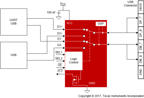
TS5USBC400 USB/UART switch. The TS5USBC400 is used to switch signals between the USB path, which goes to the baseband or application processor, or the UART path, which goes to debug port. The TS5USBC400 has internal 6-MΩ pull-down resistors on SEL1, SEL2, and OE. The pull-down on SEL1 and SEL2 pins ensure the D1+/D1- channel is selected by default. The pull-down on OE enables the switch when power is applied.
 Figure 17. Typical TS5USBC400 Application
9.2.1 Design Requirements
Design requirements of USB 1.0,1.1, and 2.0 standards must be followed. The TS5USBC400 has internal 6-MΩ pulldown resistors on SEL1, SEL2, and OE, so no external resistors are required on the logic pins. The internal pull-down resistor on SEL1 and SEL2 pins ensures the D1+ and D1- channels are selected by default. The internal pull-down resistor on OE enables the switch when power is applied to VCC.
9.2.2 Detailed Design Procedure
The TS5USBC400can be properly operated without any external components. However, TI recommends that unused pins must be connected to ground through a 50-Ω resistor to prevent signal reflections back into the device. TI does recommend a 100nF bypass capacitor placed close to TS5USBC400 VCC pin.
9.2.3 Application Curves
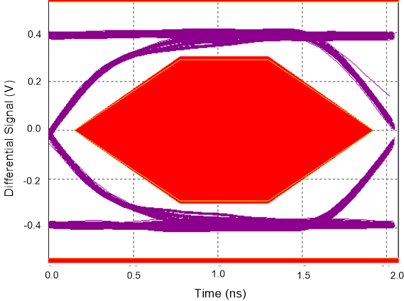
 Figure 18. High Speed Eye Diagram With TS5USBC400
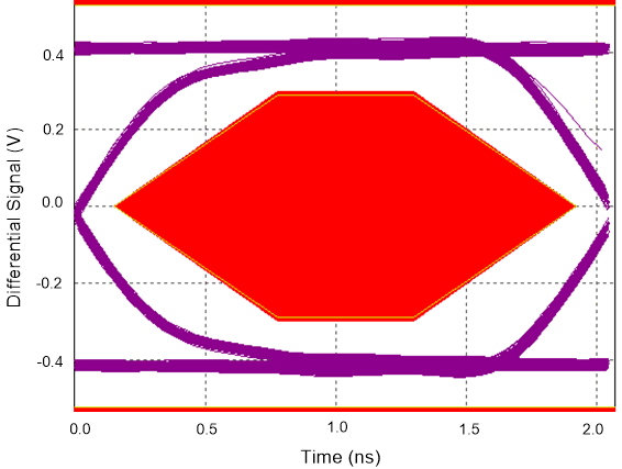
 Figure 19. High Speed Eye Diagram Without TS5USBC400