JAJSDU3A September 2017 – September 2017 TS5USBC402
PRODUCTION DATA.
- 1 特長
- 2 アプリケーション
- 3 概要
- 4 改訂履歴
- 5 Pin Configuration and Functions
- 6 Specifications
- 7 Parameter Measurement Information
- 8 Detailed Description
- 9 Application and Implementation
- 10Power Supply Recommendations
- 11Layout
- 12デバイスおよびドキュメントのサポート
- 13メカニカル、パッケージ、および注文情報
パッケージ・オプション
デバイスごとのパッケージ図は、PDF版データシートをご参照ください。
メカニカル・データ(パッケージ|ピン)
- YFP|12
サーマルパッド・メカニカル・データ
発注情報
7 Parameter Measurement Information
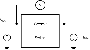
Channel ON, RON = V/ISINK
Figure 2. ON-State Resistance (RON)
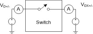 Figure 3. Off Leakage
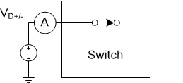 Figure 4. On Leakage
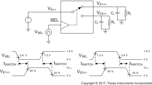
1. All input pulses are supplied by generators having the following characteristics: PRR ≤ 10 MHz, ZO = 50 Ω, tr < 500 ps, tf < 500 ps.
2. CL includes probe and jig capacitance.
Figure 5. tSWITCH Timing

1. All input pulses are supplied by generators having the following characteristics: PRR ≤ 10 MHz, ZO = 50 Ω, tr < 500 ps, tf < 500 ps.
2. CL includes probe and jig capacitance.
Figure 6. tON, tOFF for OE
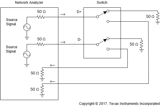 Figure 7. Off Isolation
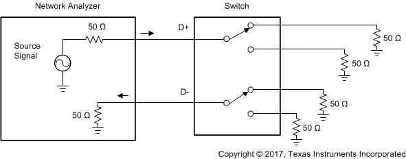 Figure 8. Cross Talk
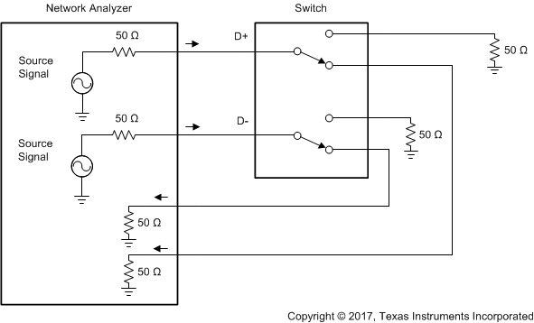 Figure 9. BW and Insertion Loss
 Figure 10. tEN_OVP and tDIS_OVP Timing Diagram

1. All input pulses are supplied by generators having the following characteristics: PRR ≤ 10 MHz, ZO = 50 Ω, tr < 500 ps, tf < 500 ps.
2. CL includes probe and jig capacitance.
Figure 11. tPD
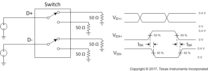
1. All input pulses are supplied by generators having the following characteristics: PRR ≤ 10 MHz, ZO = 50 Ω, tr < 500 ps, tf < 500 ps.
2. CL includes probe and jig capacitance.
Figure 12. tSK