JAJSF24C March 2018 – July 2024 TUSB1002A
PRODUCTION DATA
- 1
- 1 特長
- 2 アプリケーション
- 3 概要
- 4 Pin Configuration and Functions
- 5 Specifications
-
6 Detailed Description
- 6.1 Overview
- 6.2 Functional Block Diagram
- 6.3
Feature Description
- 6.3.1 4-Level Control Inputs
- 6.3.2 Linear Equalization
- 6.3.3 Adjustable VOD Linear Range and DC Gain
- 6.3.4 USB3.2 Dual Channel Operation (MODE = “F”)
- 6.3.5 USB3.2 Single Channel Operation (MODE = “1”)
- 6.3.6 PCIe/SATA/SATA Express Redriver Operation (MODE = “R”; CFG1 = "0"; CFG2 = "0" )
- 6.3.7 Basic Redriver Operation (MODE = “0”)
- 6.4 Device Functional Modes
- 6.5 U0 Mode
- 6.6 U1 Mode
- 6.7 U2/U3 Mode
- 7 Application and Implementation
- 8 Device and Documentation Support
- 9 Revision History
- 10Mechanical, Packaging, and Orderable Information
パッケージ・オプション
デバイスごとのパッケージ図は、PDF版データシートをご参照ください。
メカニカル・データ(パッケージ|ピン)
- RGE|24
サーマルパッド・メカニカル・データ
- RGE|24
発注情報
5.7 Switching Characteristics
over operating free-air temperature and voltage range (unless otherwise noted)
| PARAMETER | TEST CONDITIONS | MIN | TYP | MAX | UNIT | |
|---|---|---|---|---|---|---|
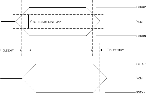
| tIDLEEntry | Delay from U0 to electrical idle | VCC = 3.0V; EN = 1; See Figure 5-1 | 150 | ps | ||
| tIDLEEntry_U1 | U1 exit time. Break in electrical idle to transmission of LFPS. | VCC = 3.0V; EN = 1; See Figure 5-1 | 150 | ps | ||
| tIDLEEntry_U2U3 | U2/U3 exit time; Break in electrical idle to transmission of LFPS | VCC = 3.0V; EN = 1; See Figure 5-1 | 6 | µs | ||
| tDIFF_DLY | Differential propagation delay | VCC = 3.0V; EN = 1; | 150 | ps | ||
| tPWRUP_ACTIVE | Time from assertion of EN to device active and performing Rx.Detect on both ports | VCC = 3.0V; EN = 1; | 8 | ms | ||
| tTX_RISE_FALL | Transmitter rise/fall time | VCC = 3.3V; EN = 1; 10Gbps; 20% to 80% of differential output; 1200mVpp linear range setting; Fast Input rise/fall time; | 27 | ps | ||
| tRF_MISMATCH | Transmitter rise/fall mismatch | VCC = 3.3V; EN = 1; 10Gbps; 20% to 80% of differential output; 1200mVpp linear range setting; 1000mVpp VID | .6 | ps | ||
| tTX_DJ | Transmitter residual deterministic jitter | VCC = 3.3V; EN = 1; 10Gbps; 1200mVpp linear range setting; Input channel loss of 12dB; Output channel loss of 1.5dB; Optimized EQ; | 0.05 | UI | ||
 Figure 5-1 Idle
Entry and Exit Latency
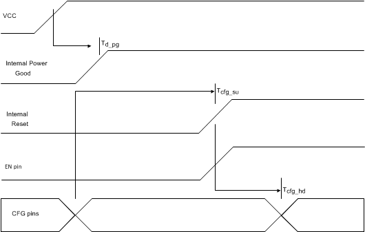
 Figure 5-2 Power-Up
Diagram