JAJSDH9D August 2017 – May 2019 TUSB1042I
PRODUCTION DATA.
- 1 特長
- 2 アプリケーション
- 3 概要
- 4 改訂履歴
- 5 Pin Configuration and Functions
-
6 Specifications
- 6.1 Absolute Maximum Ratings
- 6.2 ESD Ratings
- 6.3 Recommended Operating Conditions
- 6.4 Thermal Information
- 6.5 Power Supply Characteristics
- 6.6 DC Electrical Characteristics
- 6.7 AC Electrical Characteristics
- 6.8 DCI Specific Electrical Characteristics
- 6.9 Timing Requirements
- 6.10 Switching Characteristics
- 6.11 Typical Characteristics
- 7 Parameter Measurement Information
-
8 Detailed Description
- 8.1 Overview
- 8.2 Functional Block Diagram
- 8.3 Feature Description
- 8.4 Device Functional Modes
- 8.5 Programming
- 8.6 Register Maps
- 9 Application and Implementation
- 10Power Supply Recommendations
- 11Layout
- 12デバイスおよびドキュメントのサポート
- 13メカニカル、パッケージ、および注文情報
9.2.2 Detailed Design Procedure
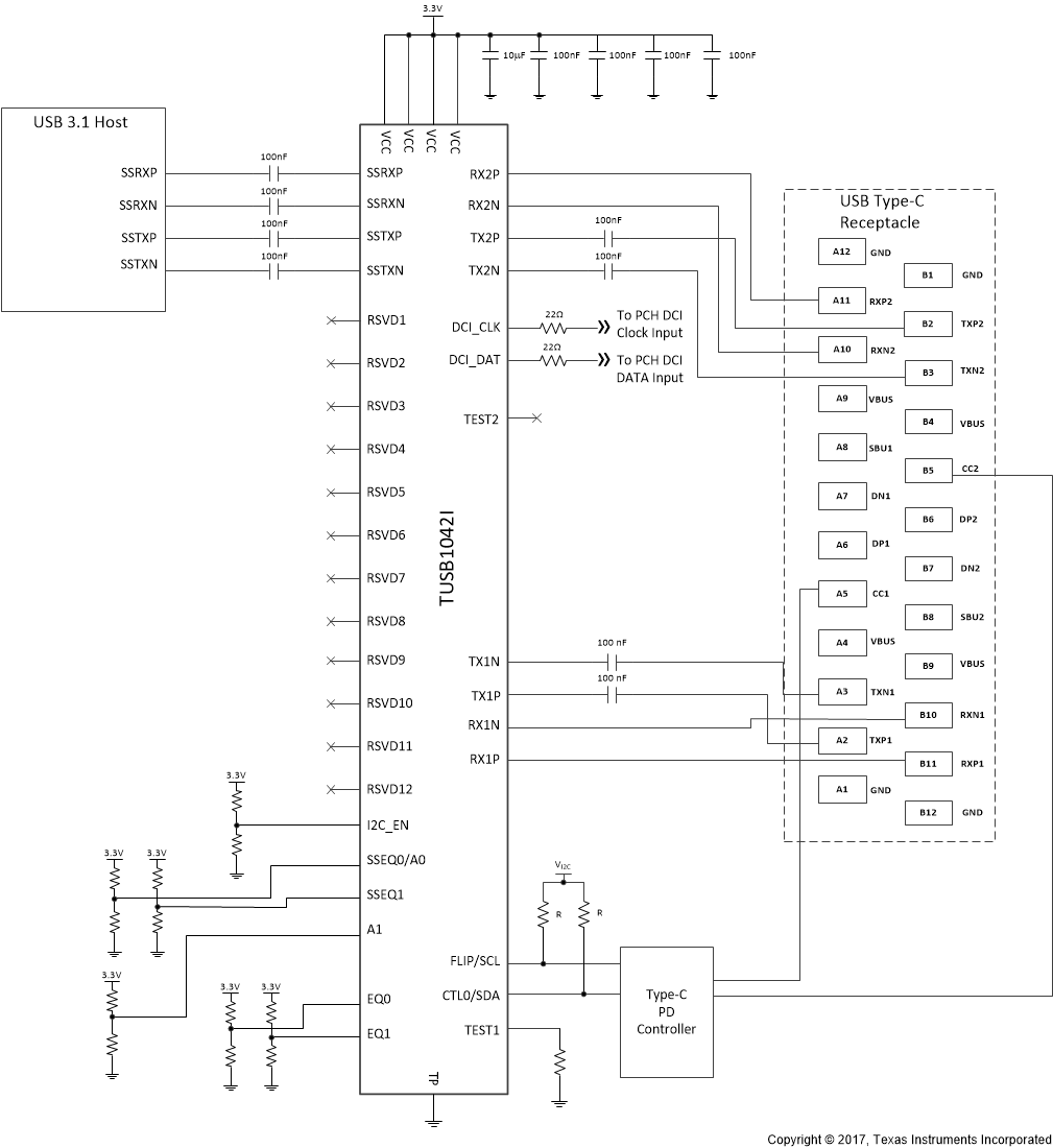
A typical usage of the TUSB1042I device is shown in Figure 20. The device can be controlled either through its GPIO pins or through its I2C interface. In the example shown below, a Type-C PD controller is used to configure the device through the I2C interface. When configured for I2C mode, pins 29 (DCI_DAT) and 32 (DCI_CLK) can be used for the DCI interface. In I2C mode, the equalization settings for each receiver can be independently controlled through I2C registers. For this reason, all of the equalization pins (EQ[1:0] and SSEQ[1:0]) can be left unconnected. If these pins are left unconnected, the TUSB1042I 7-bit I2C slave address will be 0x12 because both A1 and SSEQ0/A0 will be at pin level "F". If a different I2C slave address is desired, A1 and SSEQ0/A0 pins should be set to a level which produces the desired I2C slave address.
 Figure 20. Application Circuit