JAJSEV7C March   2018  – September 2019 TUSB1064

PRODUCTION DATA.  

  1. 特長
  2. アプリケーション
  3. 概要
    1.     Device Images
      1.      概略回路図
      2.      TUSB1064 使用事例
  4. 改訂履歴
  5. Pin Configuration and Functions
    1.     Pin Functions
  6. Specifications
    1. 6.1 Absolute Maximum Ratings
    2. 6.2 ESD Ratings
    3. 6.3 Recommended Operating Conditions
    4. 6.4 Thermal Information
    5. 6.5 ELECTRICAL CHARACTERISTICS
    6. 6.6 Switching Characteristics
    7. 6.7 Timing Requirements
    8. 6.8 Typical Characteristics
  7. Parameter Measurement Information
  8. Detailed Description
    1. 8.1 Overview
    2. 8.2 Functional Block Diagram
    3. 8.3 Feature Description
      1. 8.3.1 USB 3.1
      2. 8.3.2 DisplayPort
      3. 8.3.3 4-level Inputs
      4. 8.3.4 Receiver Linear Equalization
    4. 8.4 Device Functional Modes
      1. 8.4.1 Device Configuration in GPIO Mode
      2. 8.4.2 Device Configuration In I2C Mode
      3. 8.4.3 DisplayPort Mode
      4. 8.4.4 Linear EQ Configuration
      5. 8.4.5 USB3.1 Modes
      6. 8.4.6 Operation Timing – Power Up
    5. 8.5 Programming
    6. 8.6 Register Maps
      1. 8.6.1 General Register (address = 0x0A) [reset = 00000001]
        1. Table 11. General Registers
      2. 8.6.2 DisplayPort Control/Status Registers (address = 0x10) [reset = 00000000]
        1. Table 12. DisplayPort Control/Status Registers (0x10)
      3. 8.6.3 DisplayPort Control/Status Registers (address = 0x11) [reset = 00000000]
        1. Table 13. DisplayPort Control/Status Registers (0x11)
      4. 8.6.4 DisplayPort Control/Status Registers (address = 0x12) [reset = 00000000]
        1. Table 14. DisplayPort Control/Status Registers (0x12)
      5. 8.6.5 DisplayPort Control/Status Registers (address = 0x13) [reset = 00000000]
        1. Table 15. DisplayPort Control/Status Registers (0x13)
      6. 8.6.6 USB3.1 Control/Status Registers (address = 0x20) [reset = 00000000]
        1. Table 16. USB3.1 Control/Status Registers (0x20)
      7. 8.6.7 USB3.1 Control/Status Registers (address = 0x21) [reset = 00000000]
        1. Table 17. USB3.1 Control/Status Registers (0x21)
      8. 8.6.8 USB3.1 Control/Status Registers (address = 0x22) [reset = 00000000]
        1. Table 18. USB3.1 Control/Status Registers (0x22)
  9. Application and Implementation
    1. 9.1 Application Information
    2. 9.2 Typical Application
      1. 9.2.1 Design Requirements
      2. 9.2.2 Detailed Design Procedure
      3. 9.2.3 Support for DisplayPort UFP_D Pin Assignment E
      4. 9.2.4 PCB Insertion Loss Curves
    3. 9.3 System Examples
      1. 9.3.1 USB 3.1 Only
      2. 9.3.2 USB 3.1 and 2 Lanes of DisplayPort
      3. 9.3.3 DisplayPort Only
  10. 10Power Supply Recommendations
  11. 11Layout
    1. 11.1 Layout Guidelines
    2. 11.2 Layout Example
  12. 12デバイスおよびドキュメントのサポート
    1. 12.1 ドキュメントの更新通知を受け取る方法
    2. 12.2 コミュニティ・リソース
    3. 12.3 商標
    4. 12.4 静電気放電に関する注意事項
    5. 12.5 Glossary
  13. 13メカニカル、パッケージ、および注文情報

パッケージ・オプション

メカニカル・データ(パッケージ|ピン)
サーマルパッド・メカニカル・データ
発注情報

DisplayPort Only

The TUSB1064 operates in 4 Lanes of DisplayPort only mode when the CTL1 pin is high and CTL0 pin is low.
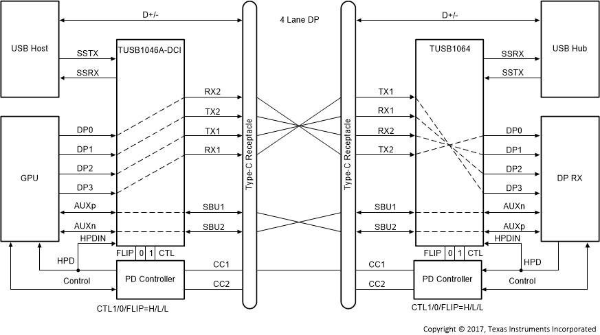
TUSB1064 TUSB1064_DCI_Four_Lane_DP_NoFlip.gifFigure 35. Four Lane DP – No Flip (CTL1 = H, CTL0 = L, FLIP = L)
TUSB1064 TUSB1064_DCI_Four_Lane_DP_Flip.gifFigure 36. Four Lane DP – With Flip (CTL1 = H, CTL0 = L, FLIP = H)