SLLSEL4A September 2014 – October 2014 TUSB1210-Q1
PRODUCTION DATA.
- 1 Features
- 2 Applications
- 3 Description
- 4 Revision History
- 5 Pin Configuration and Functions
-
6 Specifications
- 6.1 Absolute Maximum Ratings
- 6.2 Handling Ratings
- 6.3 Recommended Operating Conditions
- 6.4 Thermal Information
- 6.5 Analog I/O Electrical Characteristics
- 6.6 Digital I/O Electrical Characteristics
- 6.7 Digital IO Pins (Non-ULPI)
- 6.8 PHY Electrical Characteristics
- 6.9 Pullup/Pulldown Resistors
- 6.10 OTG Electrical Characteristics
- 6.11 Power Characteristics
- 6.12 Switching Characteristics
- 6.13 Timing Requirements
- 6.14 Typical Characteristics
-
7 Detailed Description
- 7.1 Overview
- 7.2 Functional Block Diagram
- 7.3 Feature Description
- 7.4 Device Functional Modes
- 7.5
Register Map
- 7.5.1 VENDOR_ID_LO
- 7.5.2 VENDOR_ID_HI
- 7.5.3 PRODUCT_ID_LO
- 7.5.4 PRODUCT_ID_HI
- 7.5.5 FUNC_CTRL
- 7.5.6 FUNC_CTRL_SET
- 7.5.7 FUNC_CTRL_CLR
- 7.5.8 IFC_CTRL
- 7.5.9 IFC_CTRL_SET
- 7.5.10 IFC_CTRL_CLR
- 7.5.11 OTG_CTRL
- 7.5.12 OTG_CTRL_SET
- 7.5.13 OTG_CTRL_CLR
- 7.5.14 USB_INT_EN_RISE
- 7.5.15 USB_INT_EN_RISE_SET
- 7.5.16 USB_INT_EN_RISE_CLR
- 7.5.17 USB_INT_EN_FALL
- 7.5.18 USB_INT_EN_FALL_SET
- 7.5.19 USB_INT_EN_FALL_CLR
- 7.5.20 USB_INT_STS
- 7.5.21 USB_INT_LATCH
- 7.5.22 DEBUG
- 7.5.23 SCRATCH_REG
- 7.5.24 SCRATCH_REG_SET
- 7.5.25 SCRATCH_REG_CLR
- 7.5.26 VENDOR_SPECIFIC1
- 7.5.27 VENDOR_SPECIFIC1_SET
- 7.5.28 VENDOR_SPECIFIC1_CLR
- 7.5.29 VENDOR_SPECIFIC2
- 7.5.30 VENDOR_SPECIFIC2_SET
- 7.5.31 VENDOR_SPECIFIC2_CLR
- 7.5.32 VENDOR_SPECIFIC1_STS
- 7.5.33 VENDOR_SPECIFIC1_LATCH
- 7.5.34 VENDOR_SPECIFIC3
- 7.5.35 VENDOR_SPECIFIC3_SET
- 7.5.36 VENDOR_SPECIFIC3_CLR
- 8 Application and Implementation
- 9 Power Supply Recommendations
- 10Layout
- 11Device and Documentation Support
- 12Mechanical, Packaging, and Orderable Information
パッケージ・オプション
メカニカル・データ(パッケージ|ピン)
- RHB|32
サーマルパッド・メカニカル・データ
- RHB|32
発注情報
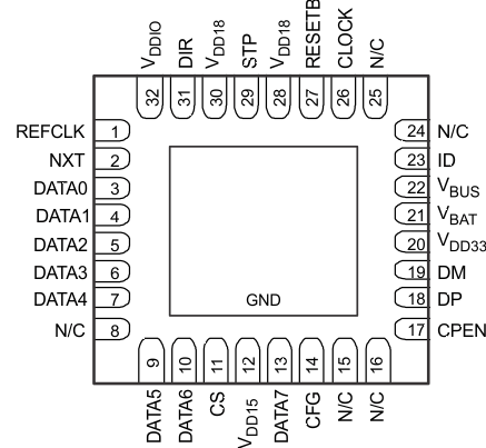
5 Pin Configuration and Functions
RHB Package
Top View

Pin Functions
| PIN | A/D | TYPE | LEVEL | DESCRIPTION | |
|---|---|---|---|---|---|
| NAME | NO. | ||||
| CFG | 14 | D | I | VDDIO | REFCLK clock frequency configuration pin. Two frequencies are supported: 19.2 MHz when 0, or 26 MHz when 1. |
| CLOCK | 26 | D | O | VDDIO | ULPI 60 MHz clock on which ULPI data is synchronized. Two modes are possible: Input Mode: CLOCK defaults as an input. Output Mode: When an input clock is detected on REFCLK pin (after 4 rising edges) then CLOCK will change to an output. |
| CPEN | 17 | D | O | VDD33 | CMOS active-high digital output control of external 5V VBUS supply |
| CS | 11 | D | I | VDDIO | Active-high chip select pin. When low the IC is in power down and ULPI bus is tri-stated. When high normal operation. Tie to VDDIO if unused. |
| DATA0 | 3 | D | I/O | VDDIO | ULPI DATA input/output signal 0 synchronized to CLOCK |
| DATA1 | 4 | D | I/O | VDDIO | ULPI DATA input/output signal 1 synchronized to CLOCK |
| DATA2 | 5 | D | I/O | VDDIO | ULPI DATA input/output signal 2 synchronized to CLOCK |
| DATA3 | 6 | D | I/O | VDDIO | ULPI DATA input/output signal 3 synchronized to CLOCK |
| DATA4 | 7 | D | I/O | VDDIO | ULPI DATA input/output signal 4 synchronized to CLOCK |
| DATA5 | 9 | D | I/O | VDDIO | ULPI DATA input/output signal 5 synchronized to CLOCK |
| DATA6 | 10 | D | I/O | VDDIO | ULPI DATA input/output signal 6 synchronized to CLOCK |
| DATA7 | 13 | D | I/O | VDDIO | ULPI DATA input/output signal 7 synchronized to CLOCK |
| DIR | 31 | D | O | VDDIO | ULPI DIR output signal |
| DM | 19 | A | I/O | VDD33 | DM pin of the USB connector |
| DP | 18 | A | I/O | VDD33 | DP pin of the USB connector |
| ID | 23 | A | I/O | VDD33 | Identification (ID) pin of the USB connector |
| N/C | 8 | – | – | VDDIO | No connect |
| N/C | 15,16, 24, 24 | – | – | – | No connect |
| NXT | 2 | D | O | VDDIO | ULPI NXT output signal |
| REFCLK | 1 | A | I | 3.3 V | VDD33 Reference clock input (square-wave only). Tie to GND when pin 26 (CLOCK) is required to be Input mode. Connect to square-wave reference clock of amplitude in the range of 3 V to 3.6 V when Pin 26 (CLOCK) is required to be Output mode. See pin 14 (CFG) description for REFCLK input frequency settings. |
| RESETB | 27 | D | I | VDDIO | When low, all digital logic (except 32 kHz logic required for power up sequencing) including registers are reset to their default values, and ULPI bus is tri-stated. When high, normal USB operation. |
| STP | 29 | D | I | VDDIO | ULPI STP input signal |
| VBAT | 21 | A | power | VBAT | Input supply voltage or battery source |
| VBUS | 22 | A | power | VBUS | VBUS pin of the USB connector |
| VDD15 | 12 | A | power | 1.5-V internal LDO output. Connect to external filtering capacitor. | |
| VDD18 | 28, 30 | A | power | VDD18 | External 1.8-V supply input. Connect to external filtering capacitor. |
| VDD33 | 20 | A | power | VDD33 | 3.3-V internal LDO output. Connect to external filtering capacitor. |
| VDDIO | 32 | A | I | VDDIO | External 1.8V supply input for digital I/Os. Connect to external filtering capacitor. |
| GND | Thermal Pad | A | power | -- | Reference Ground |