JAJSR79
September 2023
TUSB211A
PRODUCTION DATA
1
1
特長
2
アプリケーション
3
概要
4
Revision History
5
Pin Configuration and Functions
6
Specifications
6.1
Absolute Maximum Ratings
6.2
ESD Ratings
6.3
Recommended Operating Conditions
6.4
Thermal Information
6.5
Electrical Characteristics
6.6
Switching Characteristics
6.7
Timing Requirements
6.8
Typical Characteristics
7
Detailed Description
7.1
Overview
7.2
Functional Block Diagram
7.3
Feature Description
7.3.1
High-Speed EQ
7.4
Device Functional Modes
7.4.1
Low-Speed (LS) Mode
7.4.2
Full-Speed (FS) Mode
7.4.3
High-Speed (HS) Mode
7.4.4
High-Speed Downstream Port Electrical Compliance Test Mode
7.4.5
Shutdown Mode
8
Application and Implementation
8.1
Application Information
8.2
Typical Application
8.2.1
Design Requirements
8.2.2
Detailed Design Procedure
8.2.2.1
Test Procedure to Construct USB High-Speed Eye Diagram
8.2.2.1.1
For a Host Side Application
8.2.2.1.2
For a Device Side Application
8.2.3
Application Curves
8.3
Power Supply Recommendations
8.4
Layout
8.4.1
Layout Guidelines
8.4.2
Layout Example
9
Device and Documentation Support
9.1
ドキュメントの更新通知を受け取る方法
9.2
サポート・リソース
9.3
Trademarks
9.4
静電気放電に関する注意事項
9.5
用語集
10
Mechanical, Packaging, and Orderable Information
パッケージ・オプション
メカニカル・データ(パッケージ|ピン)
RWB|12
MPQF391C
サーマルパッド・メカニカル・データ
発注情報
jajsr79_oa
jajsr79_pm
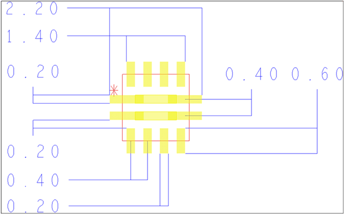
8.4.2
Layout Example
Figure 8-15
DP and DM Routing Underneath Device Package