JAJSDO7A August   2017  – September 2017 TUSB214-Q1

PRODUCTION DATA.  

  1. 特長
  2. アプリケーション
  3. 概要
  4. 改訂履歴
  5. Pin Configuration and Functions
  6. Specifications
    1. 6.1 Absolute Maximum Ratings
    2. 6.2 ESD Ratings
    3. 6.3 Recommended Operating Conditions
    4. 6.4 Thermal Information
    5. 6.5 Electrical Characteristics
    6. 6.6 Switching Characteristics
    7. 6.7 Typical Characteristics
  7. Detailed Description
    1. 7.1 Overview
    2. 7.2 Functional Block Diagram
    3. 7.3 Feature Description
      1. 7.3.1 EQ
      2. 7.3.2 DC BOOST
      3. 7.3.3 BC1.2 CDP Support
    4. 7.4 Device Functional Modes
      1. 7.4.1 Low Speed (LS) Mode
      2. 7.4.2 Full Speed (FS) Mode
      3. 7.4.3 High Speed (HS) Mode
      4. 7.4.4 Shutdown Mode
      5. 7.4.5 I2C Mode
  8. Application and Implementation
    1. 8.1 Application Information
    2. 8.2 Typical Application
      1. 8.2.1 Design Requirements
      2. 8.2.2 Detailed Design Procedure
        1. 8.2.2.1 Test Procedure to Construct USB High Speed Eye Diagram
          1. 8.2.2.1.1 For a Host Side Application
          2. 8.2.2.1.2 For a Device Side Application
      3. 8.2.3 Application Curves
  9. Power Supply Recommendations
  10. 10Layout
    1. 10.1 Layout Guidelines
    2. 10.2 Layout Example
  11. 11デバイスおよびドキュメントのサポート
    1. 11.1 ドキュメントのサポート
    2. 11.2 ドキュメントの更新通知を受け取る方法
    3. 11.3 コミュニティ・リソース
    4. 11.4 商標
    5. 11.5 静電気放電に関する注意事項
    6. 11.6 Glossary
  12. 12メカニカル、パッケージ、および注文情報

パッケージ・オプション

メカニカル・データ(パッケージ|ピン)
サーマルパッド・メカニカル・データ
発注情報

Layout

Layout Guidelines

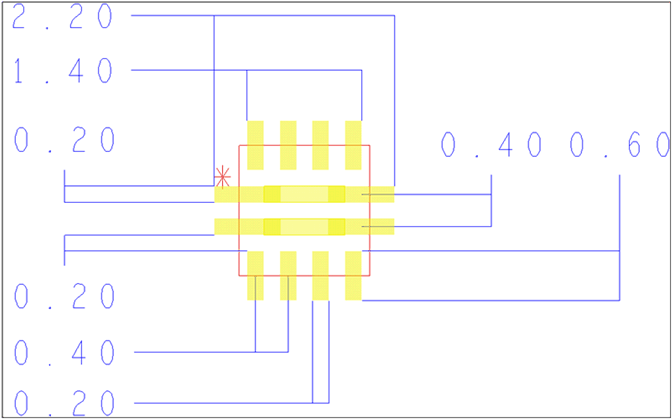
The USB signal trace must not be broken when placing TUSB214-Q1. Thus, even with the TUSB214-Q1 powered down, or not populated, the USB link is still fully operational. To avoid the need for signal vias, it is highly recommend to route the High Speed traces directly underneath the TUSB214-Q1 package, as illustrated in the PCB land pattern shown in Figure 22.

Although the land pattern shown below has matched trace width to pad width, optimal impedance control is based on the user's own PCB stack-up. It is recommended to maintain 90 Ω differential routing underneath the device.

All dimensions are in millimetres (mm).

Layout Example

TUSB214-Q1 layout_sllseo9_TUSB211.gif Figure 22. DP and DM Routing Underneath Device Package