JAJSG68A September 2018 – December 2018 TUSB217-Q1
PRODUCTION DATA.
- 1 特長
- 2 アプリケーション
- 3 概要
- 4 改訂履歴
- 5 Pin Configuration and Functions
- 6 Specifications
-
7 Detailed Description
- 7.1 Overview
- 7.2 Functional Block Diagram
- 7.3 Feature Description
- 7.4 Device Functional Modes
- 7.5 TUSB217 Registers
- 8 Application and Implementation
- 9 Power Supply Recommendations
- 10Layout
- 11デバイスおよびドキュメントのサポート
- 12メカニカル、パッケージ、および注文情報
パッケージ・オプション
デバイスごとのパッケージ図は、PDF版データシートをご参照ください。
メカニカル・データ(パッケージ|ピン)
- RGY|14
サーマルパッド・メカニカル・データ
発注情報
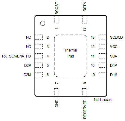
5 Pin Configuration and Functions
RGY Package
14 Pin (VQFN)
Top View

Pin Functions
| PIN | I/O | INTERNAL
PULLUP/PULLDOWN |
DESCRIPTION | |
|---|---|---|---|---|
| NAME | NO. (RGY) | |||
| BOOST | 1 | I | N/A | USB High Speed boost select via external pull down resistor.
Both edge boost and DC boost are controlled by a single pin in non-I2C mode. In I2C mode edge boost and DC boost can be individually controlled. Sampled upon power up. Does not recognize real time adjustments. Auto selects BOOST LEVEL = 3 when left floating. |
| NC | 2,3 | I | Leave unconnected | |
| RESERVED | 8 | O | Leave unconnected or connect a decoupling cap 0.1μF | |
| RX_SEN(2)/ENA_HS | 4 | I/O | N/A | In I2C mode:
Reserved for TI test purpose. In non-I2C mode: At reset: 3-level input signal RX_SEN. USB High Speed RX Sensitivity Setting to Compensate ISI Jitter H (pin is pulled high) – high RX sensitivity (high loss channel) M (pin is left floating) – medium RX sensitivity (medium loss channel) L (pin is pulled low) – low RX sensitivity (low loss channel) After reset: Output signal ENA_HS. Flag indicating that channel is in High Speed mode. Asserted upon: 1. Detection of USB-IF High Speed test fixture from an unconnected state followed by transmission of USB TEST_PACKET pattern. 2. Squelch detection following USB reset with a successful HS handshake [HS handshake is declared to be successful after single chirp J chirp K pair where each chirp is within 18 μs – 128 μs]. |
| D2P | 5 | I/O | N/A | USB High Speed positive port. |
| D2M | 6 | I/O | N/A | USB High Speed negative port. |
| GND | 7 | P | N/A | Ground |
| D1M | 9 | I/O | N/A | USB High Speed negative port.. |
| D1P | 10 | I/O | N/A | USB High Speed positive port. |
| SDA(1) | 11 | I/O | 500 kΩ PU
1.8 MΩ PD |
I2C Mode:
Bidirectional I2C data pin [7-bit I2C slave address = 0x2C]. In non I2C mode: Reserved for TI test purpose. |
| VCC | 12 | P | N/A | Supply power |
| RSTN | 14 | I | 500 kΩ PU
1.8 MΩ PD |
Device disable/enable.
Low – Device is at reset and in shutdown, and High - Normal operation. Recommend 0.1-µF external capacitor to GND to ensure clean power on reset if not driven. If the pin is driven, it must be held low until the supply voltage for the device reaches within specifications. |
| SCL(1)/CD | 13 | I/O | When RSTN asserted there is a 500 kΩ PD | In I2C mode:
I2C clock pin [I2C address = 0x2C]. Non I2C mode: After reset: Output CD. Flag indicating that a USB device is attached (connection detected). Asserted from an unconnected state upon detection of DP or DM pull-up resistor. De-asserted upon detection of disconnect. |
| Thermal Pad | TPAD | N/A | N/A | Thermal Pad is electrically not connected to device ground. Connection to board ground is optional. |
(1) Pull-up resistors for SDA and SCL pins in I2C mode should be RPull-up (depending on I2C bus voltage). If both SDA and SCL are pulled up at power-up the device enters into I2C mode.
(2) Pull-down and pull-up resistors for RX_SEN pin must follow RRXSEN1 and RRXSEN2 resistor recommendations in non I2C mode.