JAJSGA7B September   2018  – November 2021 TVS1401

PRODUCTION DATA  

  1. 特長
  2. アプリケーション
  3. 概要
  4. Revision History
  5. 概要 (続き)
  6. Device Comparison Table
  7. Pin Configuration and Functions
  8. Specifications
    1. 8.1 Absolute Maximum Ratings
    2. 8.2 ESD Ratings - JEDEC
    3. 8.3 ESD Ratings - IEC
    4. 8.4 Recommended Operating Conditions
    5. 8.5 Thermal Information
    6. 8.6 Electrical Characteristics
    7. 8.7 Typical Characteristics
  9. Detailed Description
    1. 9.1 Overview
    2. 9.2 Functional Block Diagram
    3. 9.3 Feature Description
    4. 9.4 Device Functional Modes
      1. 9.4.1 Protection Specifications
      2. 9.4.2 Reliability Testing
      3. 9.4.3 Zero Derating
      4. 9.4.4 Bidirectional Operation
      5. 9.4.5 Transient Performance
  10. 10Application and Implementation
    1. 10.1 Application Information
    2. 10.2 Typical Application
      1. 10.2.1 Design Requirements
      2. 10.2.2 Detailed Design Procedure
      3. 10.2.3 Application Curves
  11. 11Power Supply Recommendations
  12. 12Layout
    1. 12.1 Layout Guidelines
    2. 12.2 Layout Example
  13. 13Device and Documentation Support
    1. 13.1 Documentation Support
      1. 13.1.1 Related Documentation
    2. 13.2 Receiving Notification of Documentation Updates
    3. 13.3 サポート・リソース
    4. 13.4 Trademarks
    5. 13.5 Electrostatic Discharge Caution
    6. 13.6 Glossary
  14. 14Mechanical, Packaging, and Orderable Information

パッケージ・オプション

メカニカル・データ(パッケージ|ピン)
サーマルパッド・メカニカル・データ
発注情報

Typical Characteristics

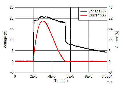
GUID-094B5E31-8774-43F1-AE51-29A80657D625-low.gifFigure 8-1 8/20 µs Surge Response at 30 A
GUID-9DDC8E2A-5456-4637-978C-33C3225632C0-low.gif
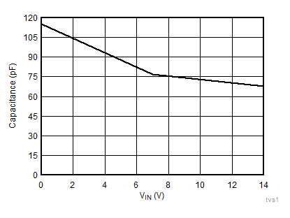
f = 1 MHz, 30 mVpp, IO to GND
Figure 8-3 Capacitance vs Voltage Bias
GUID-83F8ECE2-80C0-4BA7-9488-168CECC00AB3-low.gifFigure 8-5 Breakdown Voltage (1 mA) vs Temperature
GUID-74A78F00-1A74-4DBC-9DAD-CAEB295AB87E-low.gifFigure 8-2 8/20 µs Surge Clamping Response at 30 A
GUID-B3307624-0E2F-4390-AF55-25977D01D577-low.gifFigure 8-4 Leakage Current vs Temperature at ±14 V
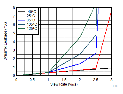
GUID-58693433-BECC-455C-8E1A-0B466D181BA6-low.gifFigure 8-6 Dynamic Leakage vs Signal Slew Rate across Temperature