SCES833B November 2011 – April 2016 TXS0206A
PRODUCTION DATA.
- 1 Features
- 2 Applications
- 3 Description
- 4 Revision History
- 5 Pin Configuration and Functions
-
6 Specifications
- 6.1 Absolute Maximum Ratings
- 6.2 ESD Ratings
- 6.3 Recommended Operating Conditions
- 6.4 Thermal Information
- 6.5 Electrical Characteristics
- 6.6 Timing Requirements—VCCA = 1.2 V ± 0.1 V
- 6.7 Timing Requirements—VCCA = 1.8 V ± 0.15 V
- 6.8 Timing Requirements—VCCA = 3.3 V ± 0.3 V
- 6.9 Switching Characteristics—VCCA = 1.2 V ± 0.1 V
- 6.10 Switching Characteristics—VCCA = 1.8 V ± 0.15 V
- 6.11 Switching Characteristics—VCCA = 3.3 V ± 0.3 V
- 6.12 Operating Characteristics —VCCA = 1.2 V
- 6.13 Operating Characteristics —VCCA = 1.8 V
- 6.14 Operating Characteristics — VCCA = 3.3 V
- 6.15 Typical Characteristics
- 7 Parameter Measurement Information
- 8 Detailed Description
- 9 Application and Implementation
- 10Power Supply Recommendations
- 11Layout
- 12Device and Documentation Support
- 13Mechanical, Packaging, and Orderable Information
8 Detailed Description
8.1 Overview
The TXS0206A is a complete application-specific voltage-translator designed to bridge the digital switching compatibility gap and interface logic threshold levels between a micrprocessor with MMC, SD, and Memory Stick™ cards. It is intended to be used in a point-to-point topology when interfacing these devices that may or may not be operating at different interface voltages.
8.2 Functional Block Diagram

8.3 Feature Description
8.3.1 Architecture
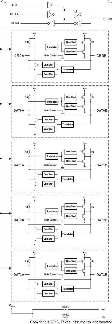
The CLKA, CLKB, and CLK-f subsystem interfaces consist of a fully-buffered voltage translator design that has its output transistors to source and sink current optimized for drive strength. CLKA is a CMOS input and therefore must not be left floating.
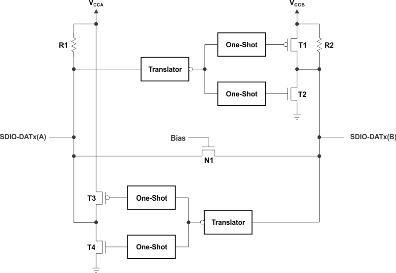
The SDIO lines comprise a semi-buffered auto-direction-sensing based translator architecture (see Figure 4) that does not require a direction-control signal to control the direction of data flow of the A to B ports (or from B to A ports).
 Figure 4. Architecture of an SDIO Switch-Type Cell
Each of these bidirectional SDIO channels independently determines the direction of data flow without a direction-control signal. Each I/O pin can be automatically reconfigured as either an input or an output, which is how this auto-direction feature is realized.
The following two key circuits are employed to facilitate the "switch-type" voltage translation function:
- Integrated pullup resistors to provide dc-bias and drive capabilities
- An N-channel pass-gate transistor topology (with a high RON of approximately 300 Ω) that ties the A-port to the B-port
- Output one-shot (O.S.) edge-rate accelerator circuitry to detect and accelerate rising edges on the A or B ports
For bidirectional voltage translation, pullup resistors are included on the device for dc current sourcing capability. The VGATE gate bias of the N-channel pass transistor is set at a level that optimizes the switch characteristics for maximum data rate as well as minimal static supply leakage. Data can flow in either direction without guidance from a control signal.
The edge-rate acceleration circuitry speeds up the output slew rate by monitoring the input edge for transitions, helping maintain the data rate through the device.
During a low-to-high signal rising-edge, the O.S. circuits turn on the PMOS transistors (T1, T3) and its associated driver output resistance of the driver is decreased to approximately 50 Ω to 70 Ω during this acceleration phase to increase the current drive capability of the driver for approximately 30 ns or 95% of the input edge, whichever occurs first. This edge-rate acceleration provides high ac drive by bypassing the internal pullup resistors during the low-to-high transition to speed up the rising-edge signal.
During a high-to-low signal falling-edge, the O.S. circuits turn on the NMOS transistors (T2, T4) and its associated driver output resistance of the driver is decreased to approximately 50 Ω to 70 Ω during this acceleration phase to increase the current drive capability of the driver for approximately 30 ns or 95% of the input edge, whichever occurs first.
To minimize dynamic ICC and the possibility of signal contention, the user should wait for the O.S. circuit to turn-off before applying a signal in the opposite direction. The worst-case duration is equal to the minimum pulse-width number provided in the Timing Requirements—VCCA = 1.2 V ± 0.1 V section of this data sheet.
Once the O.S. is triggered and switched off, both the A and B ports must go to the same state (i.e. both High or both Low) for the one-shot to trigger again. In a DC state, the output drivers maintain a Low state through the pass transistor. The output drivers maintain a High through the "smart pullup resistors" that dynamically change value based on whether a Low or a High is being passed through the SDIO lines, as follows:
- R1 and R2 values are a nominal 40 kΩ when the output is driving a low
- R1 and R2 values are a nominal 4 kΩ when the output is driving a high
- R1 and R2 values are a nominal 40 kΩ when the device is disabled via the EN pin or by pulling the either VCCA or VCCB to 0 V.
- The threshold at which the resistance changes is approximately VCCx/2
The reason for using these "smart" pullup resistors is to allow the TXS0206 to realize a lower static power consumption (when the I/Os are low), support lower VOL values for the same size pass-gate transistor, and improved simultaneous switching performance.
8.4 Device Functional Modes
Table 1 lists the functional modes of the TXS0206A.
Table 1. Function Table
| EN | TRANSLATOR I/Os |
|---|---|
| L | Disabled, pulled to VCCA, VCCB through 40 kΩ |
| H | Active |