JAJSCQ9A December 2016 – February 2019 UC1843A-SP
PRODUCTION DATA.
- 1 特長
- 2 アプリケーション
- 3 概要
- 4 改訂履歴
- 5 Device Comparison Table
- 6 Pin Configuration and Functions
- 7 Specifications
- 8 Detailed Description
- 9 Application and Implementation
- 10Power Supply Recommendations
- 11Layout
- 12デバイスおよびドキュメントのサポート
- 13メカニカル、パッケージ、および注文情報
パッケージ・オプション
メカニカル・データ(パッケージ|ピン)
サーマルパッド・メカニカル・データ
発注情報
8.3.1 UVLO
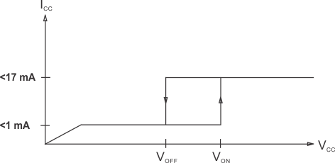
The UVLO circuit ensures that VCC is adequate to make the UC1843A-SP fully operational before enabling the output stage. Figure 5 shows that the UVLO turnon and turnoff thresholds are fixed internally at 16 V and 10 V, respectively. The 6-V hysteresis prevents VCC oscillations during power sequencing.
Figure 6 shows supply current requirements. Start-up current is < 1 mA for efficient bootstrapping from the rectified input of an off-line converter, as shown in Figure 7. During normal circuit operation, VCC is developed from auxiliary winding, WAux, with D1 and CIN. However, at start-up, CIN must be charged to 16 V through RIN. With a start-up current of 1 mA, RIN can be as large as 100 kΩ and still charge CIN when VAc = 90-V RMS (low line). Power dissipation in RIN would then be less than 350 mW even under high line (VAc = 130-V RMS) conditions.
During UVLO, the output driver is in a low state. While it does not exhibit the same saturation characteristics as normal operation, it can easily sink 1 mA, enough to ensure the MOSFET is held off.
 Figure 5. UVLO Turnon TurnOff Threshold
 Figure 7. Providing Power to the UC1843A-SP