JAJSH61A April 2019 – September 2019 UC1843B-SP
PRODUCTION DATA.
- 1 特長
- 2 アプリケーション
- 3 概要
- 4 改訂履歴
- 5 Pin Configuration and Functions
- 6 Specifications
- 7 Detailed Description
- 8 Application and Implementation
- 9 Power Supply Recommendations
- 10Layout
- 11デバイスおよびドキュメントのサポート
- 12メカニカル、パッケージ、および注文情報
パッケージ・オプション
メカニカル・データ(パッケージ|ピン)
- KGD|0
- HKU|10
サーマルパッド・メカニカル・データ
発注情報
7.3.1 UVLO
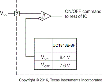
The UVLO circuit ensures that VCC is adequate to make the UC1843B-SP fully operational before enabling the output stage. Figure 5 shows that the UVLO turnon and turnoff thresholds are fixed internally at 8.4 V and 7.6 V, respectively. The 0.6-V hysteresis prevents VCC oscillations during power sequencing.
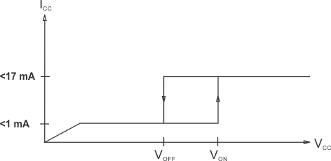
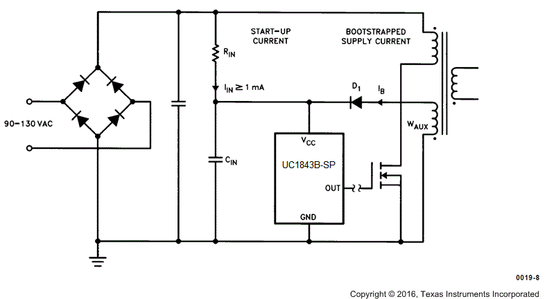
Figure 6 shows supply current requirements. Start-up current is < 1 mA for efficient bootstrapping from the rectified input of an off-line converter, as shown in Figure 7. During normal circuit operation, VCC is developed from auxiliary winding, WAux, with D1 and CIN. However, at start-up, CIN must be charged to 8.4 V through RIN. With a start-up current of 1 mA, RIN can be as large as 100 kΩ and still charge CIN when VAC = 90-V RMS (low line). Power dissipation in RIN would then be less than 350 mW even under high line (VAC = 130-V RMS) conditions.
During UVLO, the output driver is in a low state. While it does not exhibit the same saturation characteristics as normal operation, it can easily sink 1 mA, enough to ensure the MOSFET is held off. For efficient operations, an LDO can take the place of RIN and be disabled during the operation of the device.
 Figure 5. UVLO Turnon and Turnoff Threshold
NOTE:
During UVLO, the output driver is biased to sink minor amounts of current. Figure 7. Providing Power to the UC1843B-SP